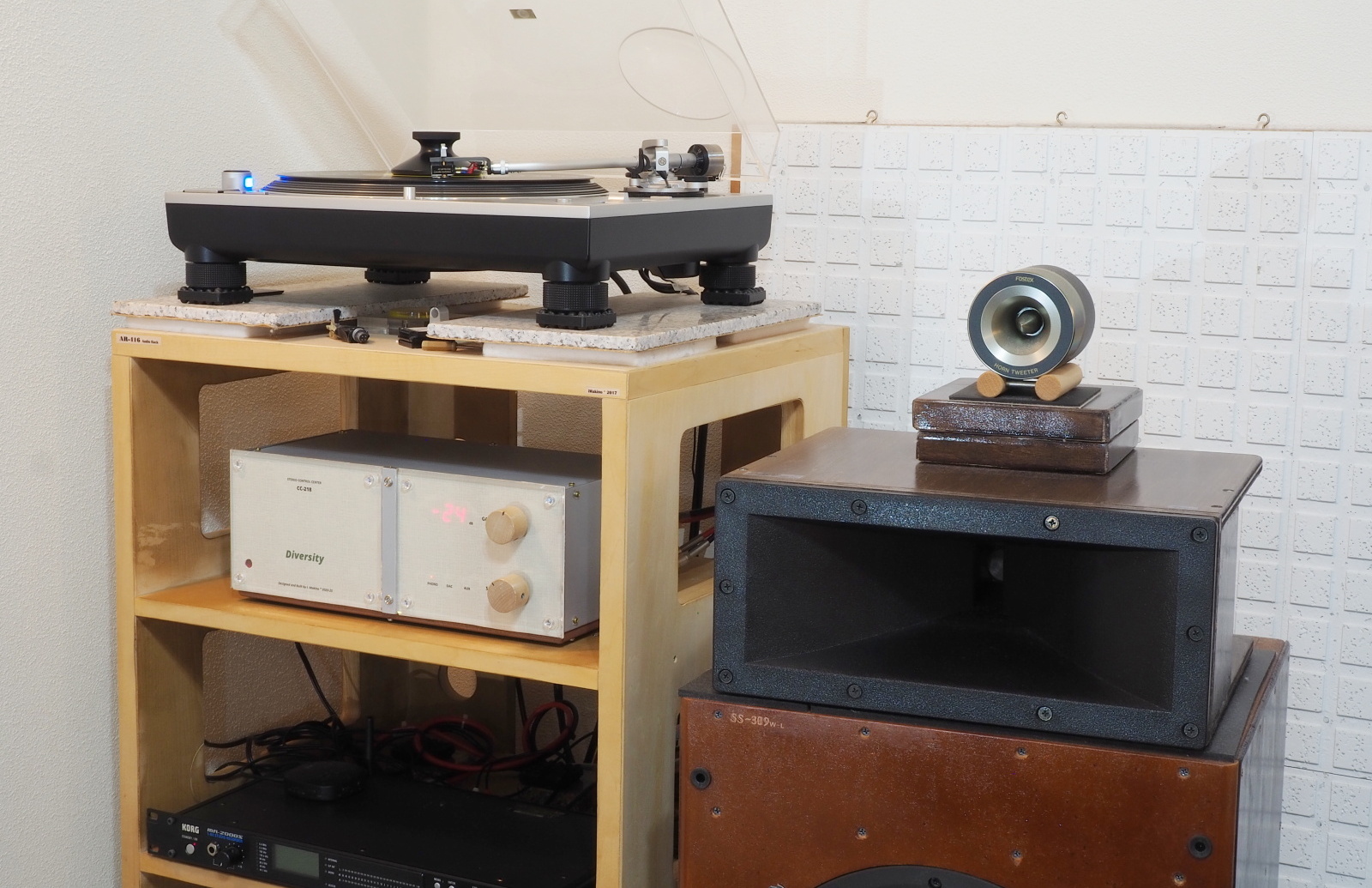
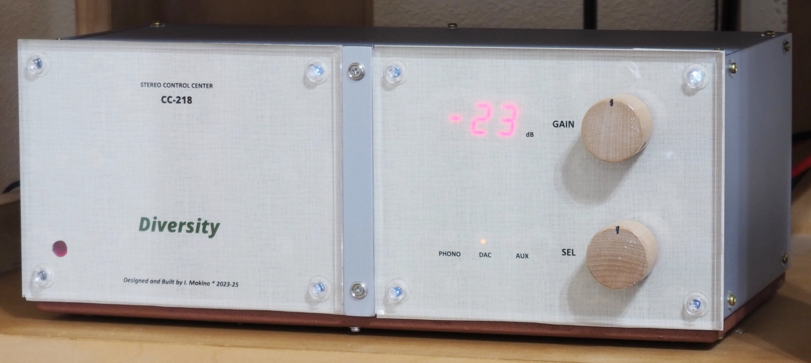
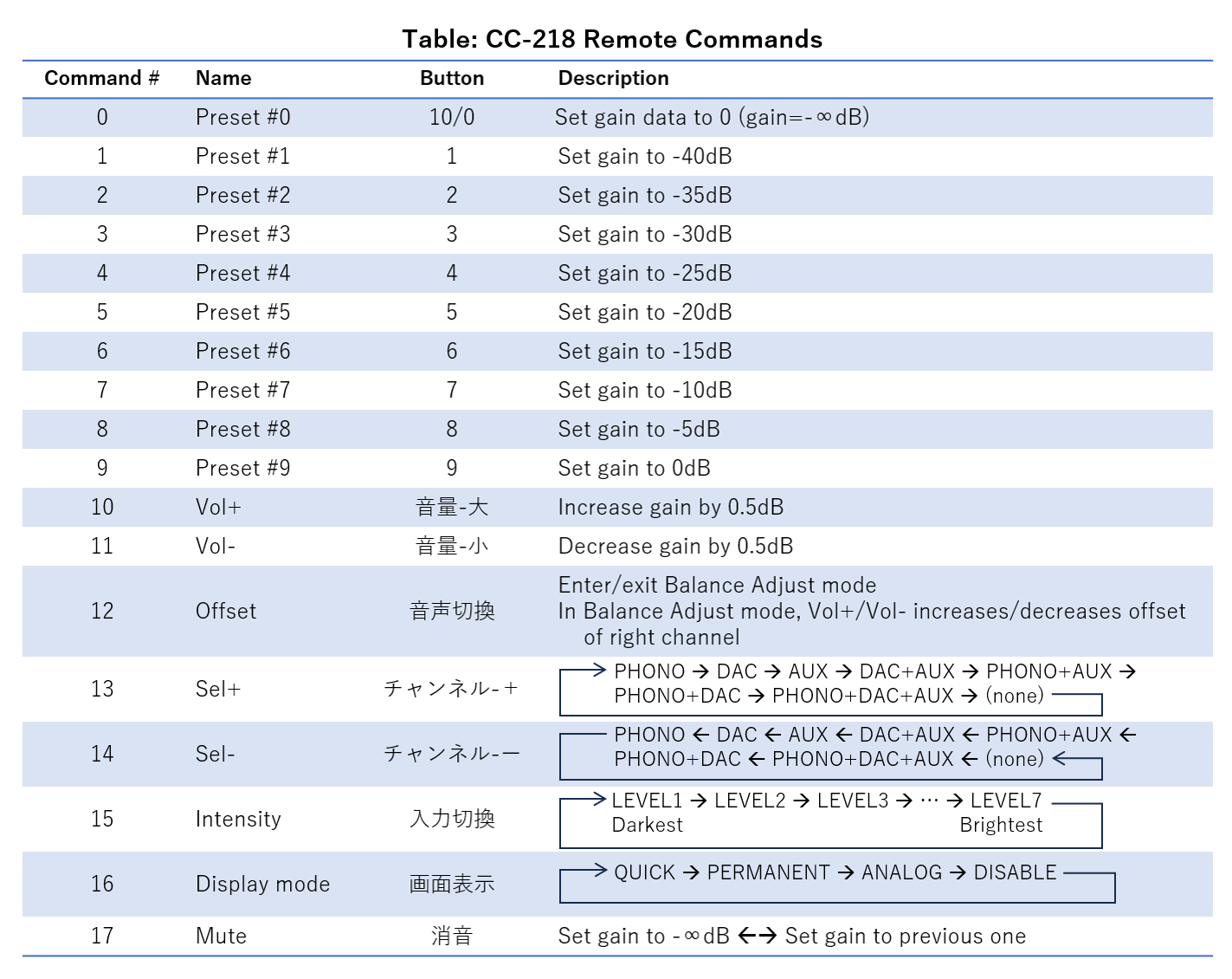
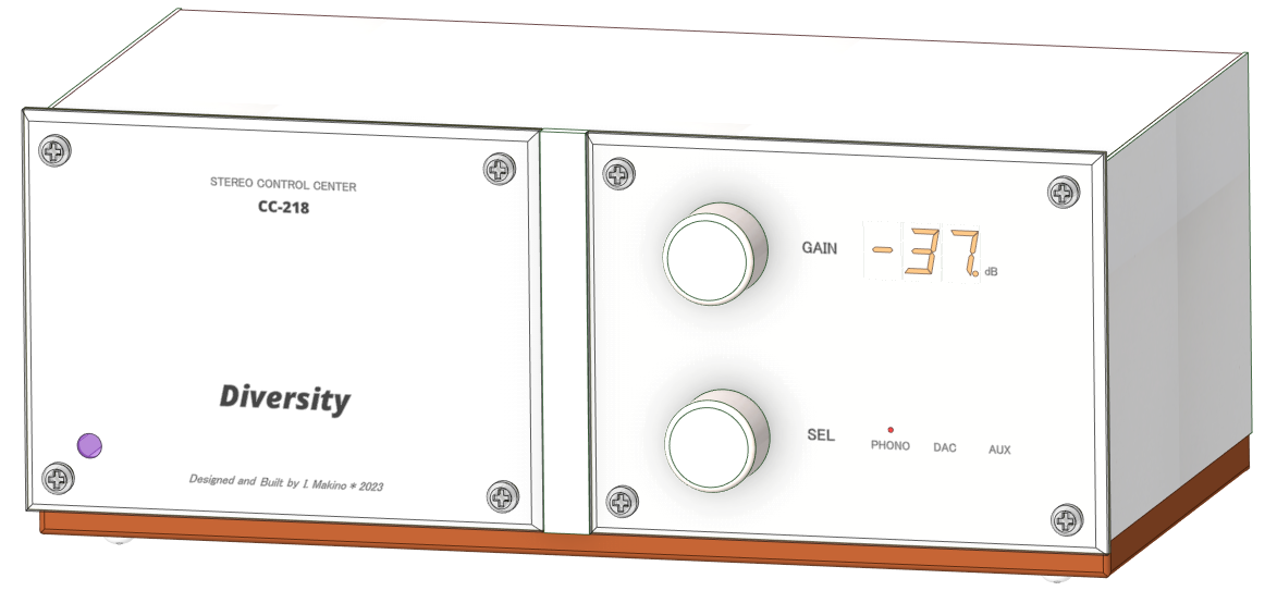
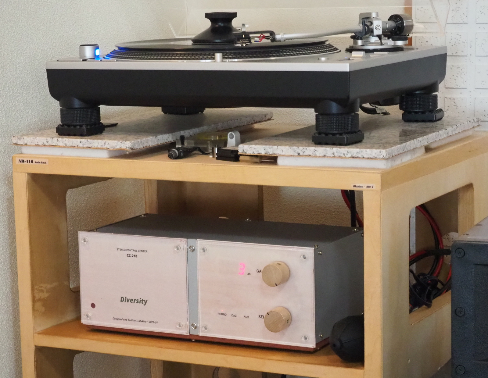
CC-218 Diversity
2025/08/06 created
2025/10/02 updated
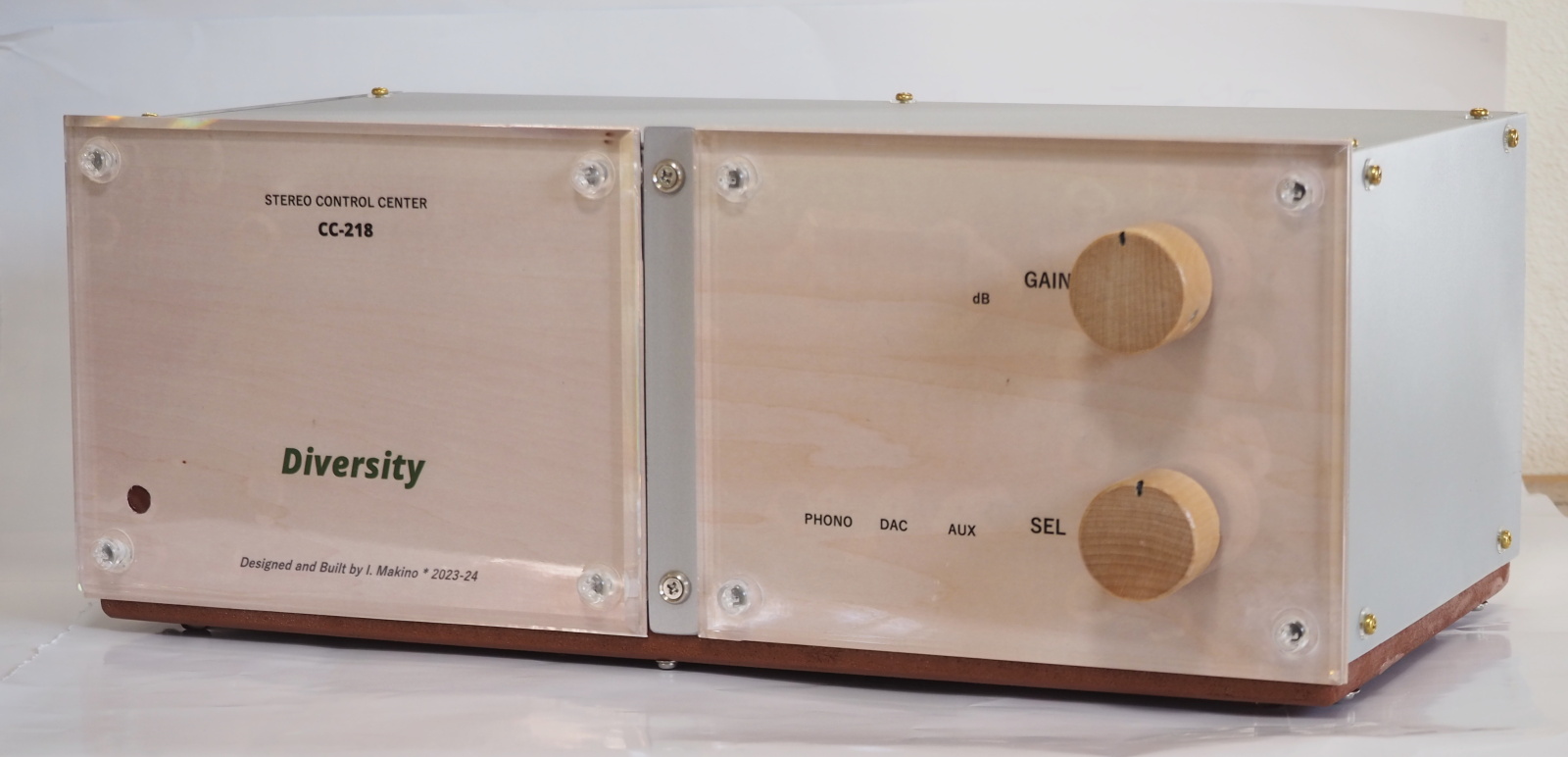
Stereo Control Center (Preamplifer)
One and only preamp that meets all of my personal requirements!
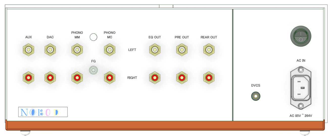
| Features | Electronic volume using TI PGA2310, Selector using shunt switching, Phono EQ for MC cartridge only, Matrix circuitry compatible with Sansui QS4 (4-channel stereo)、Detachable front panels, IR remote, Controlable by PC, DVCS support. |
|---|---|
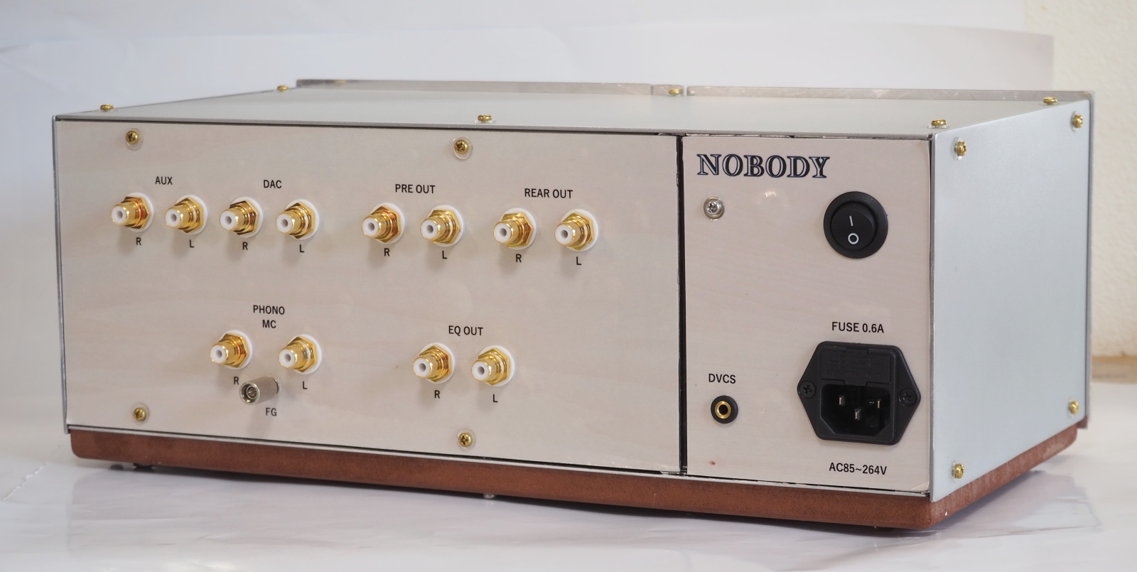
| Outline Specifications | Inputs: PHONO(MC only), LINE IN x2 (DAC, AUX). Output: PRE OUT x1, REAR OUT, EQ OUT. Maximum gain: +3dB. Frequency range: DC-160kHz (-3dB). |
| Dimension | Dimension: 360(W) x 142(H) x 190(D) mm (not including protrusions). Weight: 4.5kg (not including the power cord). |
| Cost | 106,422 JPY |
| History | Design started in May, 2023. Completed in May, 2025. Being used in Gaudi II. |
Contents:
Concept
Specifications
Design
Appearance Design
Mechanical Design
Layout and Wiring Design
Circuit Design
PCB Design
Firmware Design
Building
Measurements and Improvements
My Own Review
Summing-up
Concept
This is the preamplifier to be used in Gaudi Ver. 3.0. I named it the “Control
Center” because it has the capability to control a crossover network (hereafter
referred to as the “Xover”) and the power amplifier via the DVCS (which
I will explain later).
For me, this is my fifth self-built preamplifier (or the sixth if you count
the MV-217 as a preamplifier). Based on my past experiences, I have learned
many things and, as a result, have formed my own ideal vision. In this
project, I aimed to create my ideal preamplifier by bringing together all
of my knowledge and skills.
Top priorities in design are as follows:
- (1) Good appearance that fits with my taste and the interior of the room
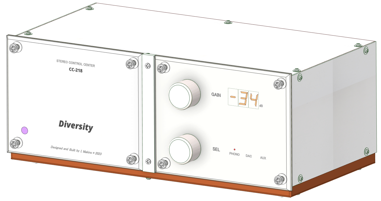
- This is a concept carried over from my previous work, the MV-217 X'tal. With the CC-218, I took this idea even further by making the front panel detachable. Since the appearance can be easily changed, it allows for applications such as changing the look to match the seasons.
- (2) Maintenance-free for 25 years
- By making the selector and volume contactless and using a sealed enclosure, the initial performance can be maintained over a long period of time. Components that deteriorate quickly with age, such as vacuum tubes, are not used.
- (3) DVCS support
- DVCS (Distributed Volume Control System) is a technology I developed myself. It is a system in which the volume control interface is built into the preamplifier, while the actual volume control circuitry is housed inside the power amplifier or the Xover. The aim is to improve the overall system’s SNR and dynamic range.
- (4) PCB
- Since electronic volume control and a digital display are used, incorporating an MCU (Microcontroller Unit) is essential. To miniaturize the control board equipped with the MCU, stabilize its operation, and reduce unwanted emissions, a PCB (Printed Circuit Board) is employed. Even for implementing the analog circuitry, using a PCB has advantages, such as stabilizing the ground potential and preventing crosstalk between signals.
- (5) Four-channel stereo
- This is one of my personal requirements. I own several QS4 records, but I have never listened to them in four-channel. For many years, I have wanted to hear their original sound.
- (6) Console feature
- By connecting CC-218 to a PC and running a terminal software application such as Tera Term on the PC, CC-218 can send status information (such as the internal state of the device or events occurring within the device) to be displayed on the application’s screen. In addition, commands can be sent from the application to change CC-218’s settings or execute its self-diagnostic program. I refer to this type of functionality as the “console feature,” and I call the PC running the terminal software the “Console.”
Nickname and Theme Music
The nickname is Diversity.
This work includes circuits operated under microcontroller control, such
as the electronic volume, as well as traditional circuits like a phono
equalizer (phono EQ), and even includes a feature of 4-ch stereo, a function
already forgotten by the general public. In addition to pursuing electrical
performance, attention has also been given to appearance and usability.
Since this work is packed with a variety of functions, it has been named
“Diversity.” These days, this word is often used in a moral or ethical
sense, but the name of this work carries no such moral meaning.
I chose Samba de Orfeu by the Ted Sommer Orchestra (LP, Ted Sommer Orchestra,
Percussive Mariachi, Solid State SS-18012) as the theme music. It’s a crossover piece that
blends jazz, Latin, samba, bossa nova, and mariachi — traditional Mexican
music.
I first heard this record when I was only ten years old, and the powerful
impression it made on me drew me deeply into the worlds of music and audio.
It’s been a lifelong favorite ever since.
--- Samba de Orfeu (TedSommer_SambaDeOrfeu_50sec.mp3) ---
Rendering
Specifications
Hardware Spec
| Inputs | PHONO (MC only), LINE x2 (DAC, AUX). |
| PHONO input | Input impedance: 100 ohm, Max input level: 13mV, Connector:Gold-plated RCA jacks. |
| LINE inputs | Input impedance: 22k ohm, Max input level: 8V (at gain =< 0dB), Connector: Gold-plated RCA jacks. |
| Outputs | PRE OUT, REAR OUT, EQ OUT. |
| PRE OUT, REAR OUT | Output impedance: 47 ohm, Load impedance: 600 ohm or higher. Maximum output level: 8V (600 ohm), Connector: Gold-plated RCA jacks. |
| EQ OUT | Output impedance: 47 ohm. Load impedance:600 ohm or higher, Max output level: 10V (600 ohm). Connector: Gold-plated RCA jacks. |
| PHONO EQ | RIAA deviation: +/-0.1dB (20Hz~20kHz). Channel deviation: +/-0.1dB (20Hz~20kHz). |
| Gain | PHONO: +66dB (1kHz). LINE: -∞dB、-60dB ~ +3dB. |
| Gain control | Panel operation: -∞dB, -60dB ~ +3dB, 1dB step. Remote control: -∞dB, -95.5dB ~ +10dB, 0.5dB step. Presets (remote): -40dB, -35dB, -30dB, ..., 0dB (5dB step). Gang error: +/-0.1dB or less. Default value: Calculated from the position of VOL (volume) knob. VOL knob rotation range: 300 deg. |
| Display of gain | Gain is displayed in dB. Display: 2-digit, 7-segment LEDs. 0.5dB (fraction) is indicated by decimal point only. '-' indicates -∞dB. Intensity: 7 steps (adjusted by remote). Display mode: 4 modes (described later) (switched by remote). |
| Frequency range | DC ~ 160kHz (-3dB) (w/ input & output LPF). DC ~ 800kHz (-1dB) (w/o input & output LPF). |
| Channel separation | 90dB or higher (@1kHz), 90dB or higher (@20kHz). |
| Distortion | Smaller than the measurable limit of Tonochi Methods. Measured data: THD: 0.008%, IMD: 0.01%. (true values are smaller than these) |
| SNR | Higher than the measurable limit of Tonochi Methods. Measured data: 67dB. (true value is higher than this). Residual noise: 70uV or lower (w/ the filter of the instrument disabled) |
| Console feature | Using PC and a terminal app on it such as Tera Term. Connection: DVCS port of CC-218-->Mini plug/D-Sub cable-->RS232C/USB cable-->USB of PC. |
| DVCS | Asynchronous serial communication: 19,200 baud, 8bit, no parity bit, w/o
flow control. Electrical charisteristic: Compliant w/ RS232C (only TX, RX and GND are used). When a DVCS device (Xover or power amp that has DVCS port) is connected, the DVCS port is assigned for DVCS feature. When PC is connected, DVCS port is assigned for console feature (automatical detection). |
| Power supply | AC100V or AC200V. (adaptor or power cord for 200V is necessary to use 200V
outlet) Voltage range: 85 ~ 264V. |
| Power dissipation | 13W (when all LEDs of display are on). 12W (when all LEDs of display are off). |
| Dimensions | Dimension: 360(W) x 142(H) x 190(D) mm (not including protrusions). Weight: 4.5kg (not including power cord). |
Level diagram
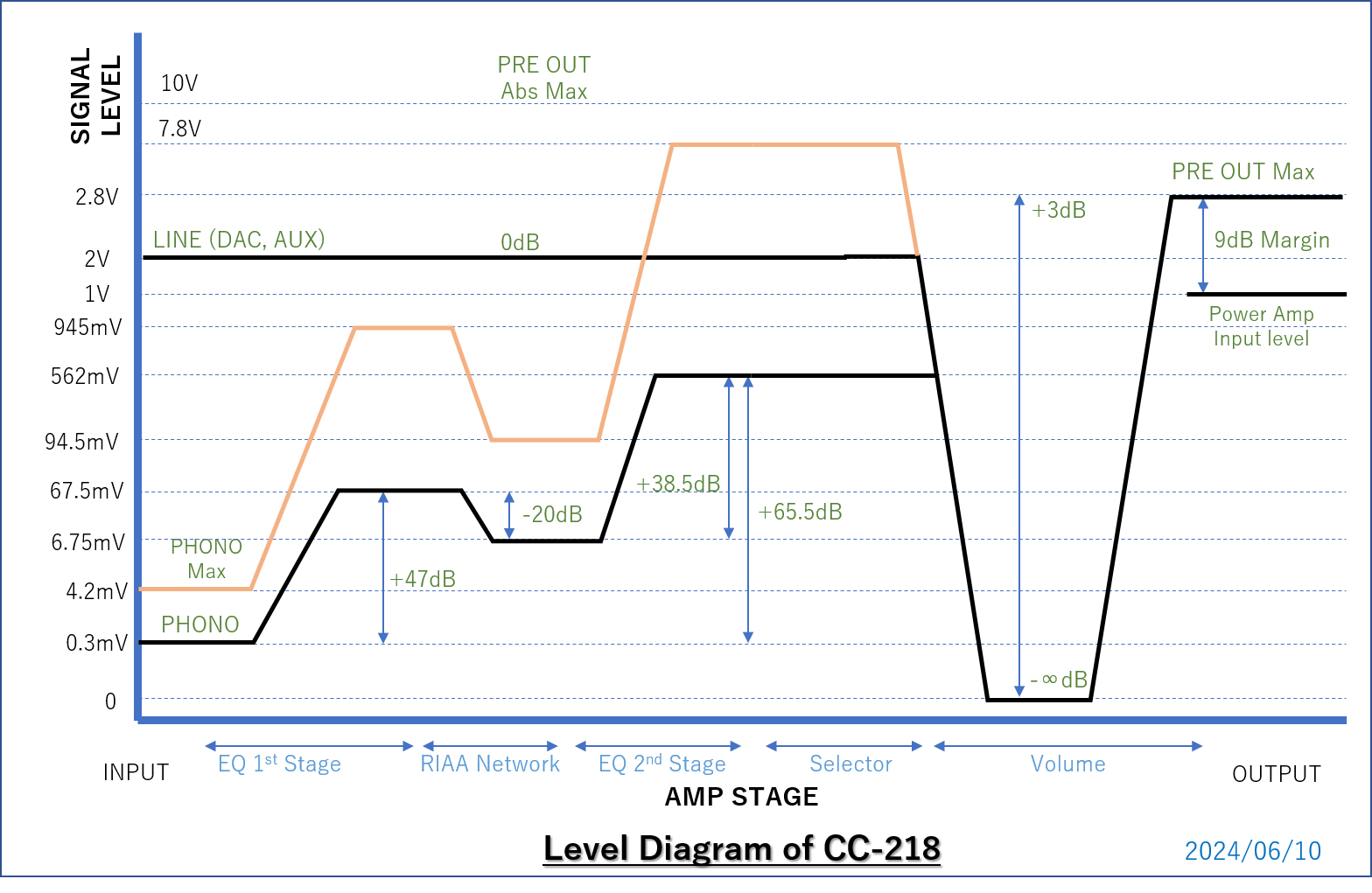
The specified maximum output level is +3dBFS (=2.8V), though, it can be extended to +10dBFS(=6.3V) by remote control.
User interface
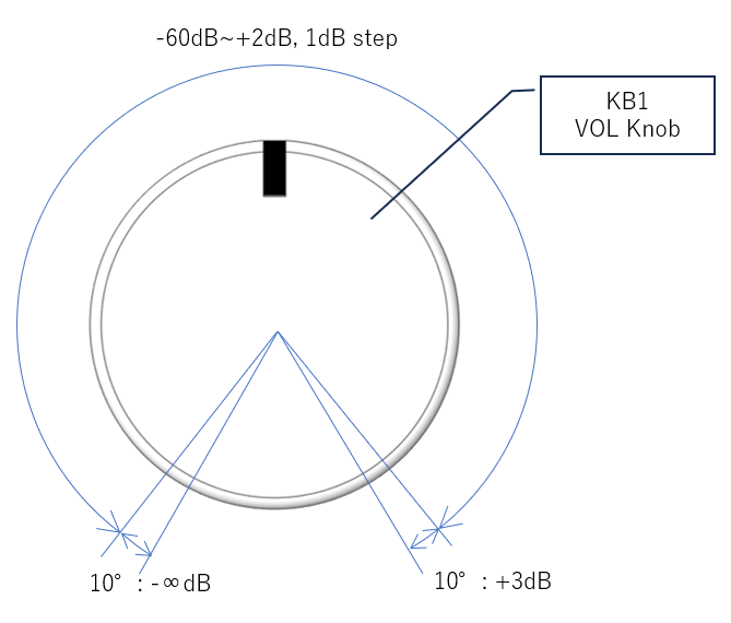
The CC-218 has a unique user interface.
To avoid causing stress for the user (myself) when playing analog discs,
a variable resistor (VR) for the volume knob instead of a rotary encoder.
The VR's rotational range is 300 degrees. This allows the user to reduce
the volume from maximum to minimum within only one second.
When lowering the stylus onto a disc or at the end of playback, the volume
must be turned down . This prevents sudden loud noise from the loudspeakers.
Such operation is far easier with VR. As for MV-217, which employs a rotary
encoder, it takes about 10 seconds to bring the volume from maximum to
minimum. By adopting VR, CC-218 achieves exactly the same operability as
a pure analog amplifier. In particular, when the display is set to 'Disable'
mode (always off), CC-218 is indistinguishable from a pure analog amplifier.
Because VR exhibits low linearity within approximately 10 degrees near
its start and end positions, the gain is fixed in those ranges. Within
10 degrees of the starting point, the gain is set to −∞ dB, and within
10 degrees of the endpoint, it is set to +3dB. Gain settings between more
than −∞ dB and less than −60 dB are considered unnecessary. Adjustment
is performed in 1dB steps.
Spec of remote
With the IR remote, the user can adjust gain in 0.5dB steps.
For explanation of 'Display mode', see "Appearance Design".
I also put a lot of thought into the mute function. I really don’t like
it when the sound just cuts off suddenly, so I set it up to fade out over
about 0.9 seconds instead. When unmuting, it fades back in the same way.
This was one of my own “picky requirements,” too.
Design
I made the appearance my top priority in this project as in MV-217 project. I planned the design steps as follows (these steps aren't separate, and overlap each other):
Appearance design ==> Mechanical design ==> Layout design ==> Circuit design ==> Firmware design.
I selected the same parts and materialsas as MV-217 which concern the appearance.
Key Parts and Materials
I selected many parts and materials I hadn't used before, as I did in the
previous project (MV-217 X'tal).
- PCB
- I used my original PCB (Print Circuit Board) for the first time in my life.
I could hardly master PCB dsign in spite of my efforts for the past few years. However, I really need a PCB in order to realize a ultra-low noise phono equalizer (Phono EQ) for MC cartridge. I had to employ PCB. I decided to use PCBs for the phono EQ and the other boards. They are all doubl-sided PCBs.
- AC/DC converter
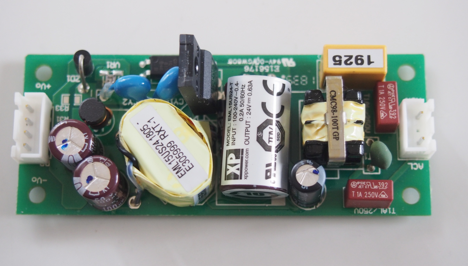 I selected XP Power's EML15USxx again, which I had selected for MV-217 and was satisfied.
Two units of EML15US24-T (24V 0.6A) for the analog circuits, and one EML15US05-S (5V 3A) for the digital circuits.
<Manufacturer's website (https://www.xppower.com/)>
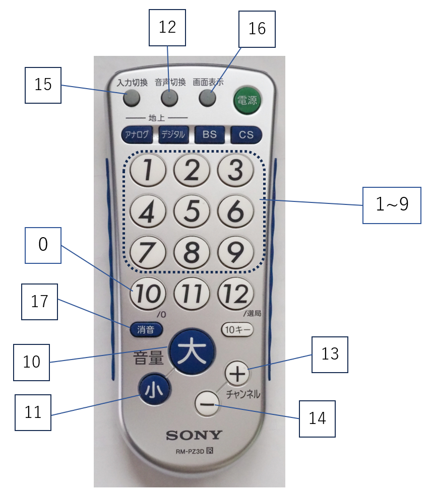
- TV remote
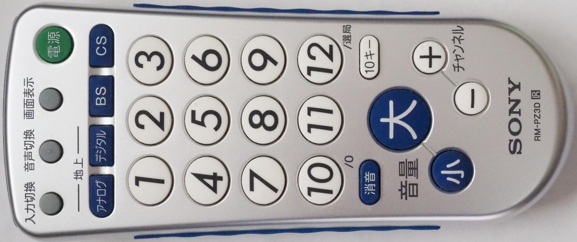 For the remote control, I chose to use a TV infrared remote. Many models
are available on the market, so it's easy to pick one that suits my preferences.
For the remote control, I chose to use a TV infrared remote. Many models
are available on the market, so it's easy to pick one that suits my preferences.
The model I selected is the Sony RM-PZ3D. For a TV remote, it has relatively few buttons, which makes it look easy to use. Since its appearance is different from the remotes for the living room TV (Sharp) and the STB (Panasonic), there's no risk of confusing them in a hurry.
The issue was how to receive the signal from this remote. According to the datasheet of an infrared receiver module, Japanese-made remotes use a Pulse Position Modulation (PPM) method with a 38 kHz carrier frequency. I decided to use the Vishay TSOP34838, which has the functionality to receive and demodulate such signals.- ICs for audio
- Electronic volume: Texas Instruments (Barr Brown) PGA3210
Ultra-low noise op amp: Linear Technology LT1115
Other op amps for audio: Texas Instruments (Barr Brown) OPA627, Texas Instruments (National Semiconductor) LME49860, LME49720 - MCU
- I chose Microchip PIC18F2520.
Its CPU is 8-bit. For controlling an amplifier, an 8-bit CPU has enough performance. I chose the PIC microcontroller because it is widely used around the world and its supply is considered stable. I also plan to use it in amplifiers I build in the future. It's an easy-to-use MCU (Microcontroller Unit) with a built-in reset circuit and clock oscillator.
CPU: 8-bit CISC(Complex Instruction Set Computer)
Clock frequency: up to 8MHz (internal clock), up to 40MHz (external clock)
Memory: program memory (flash memory) 32KB, data memory (RAM) 1.6KB, EEPROM 256B
Peripherals: Timer x4 (including capture, comparator, PWM features), Serial port x2 (USART, MCCP(I2C Bus)), 10-bit ADC, WDT, etc
New Technologies
Here are some technologies I experienced for the first time. They are already commonplace, but new to me.
- Microcontroller-based control
- In an analog preamplifier, the component most prone to causing sound quality
degradation is the volume control. Variable resistors (VR or potentiometer)
already have less-than-ideal contact quality, and they also tend to deteriorate
over time. Dual-gang VRs for stereo use also suffer from a drawback called
"gang error," caused by inconsistencies between the two potentiometer
elements.
The most practical solution is to use an electronic volume control. There are ICs specifically designed for this purpose, allowing for a single-chip implementation. However, electronic volume controls require microcontroller-based control. It was precisely the desire to use an electronic volume control that led me to adopt microcontroller control.
With microcontroller control, incorporating an infrared remote control also becomes possible.
- PCB design
- I decided to use PCBs in this project. So I had to design the PCBs for myself. As I mentioned above, it is hard for me to master PCB design techniques, though, DesignSpark PCB, a PCB CAD with excellent user interface, made it possible to design PCBs meeting my requirements.
- Infrared remote
- I had long been frustrated by the lack of a remote control on my preamps.
MV-217 was the first model I tried to equip with one, but for some reason,
it didn’t work. Since the MV-217 used a commercially available module,
I couldn’t debug it and eventually gave up. This time, both the hardware
and firmware are homemade, so I’ll make sure the remote control works.
A remote control indirectly affects sound quality. Volume and sound quality are closely related, and to achieve the best possible sound, fine volume adjustments are essential. But if you can’t adjust the volume from your listening position, you have to go back and forth between the amp and your seat. That kind of hassle makes it harder to fully enjoy the music—and as a result, it may even make the sound feel less satisfying. - I2C Bus
- It’s a widely adopted standard for internal device communication. Since it’s an interface for connecting ICs to other ICs, it was named I²C. It’s used in many types of LSI chips. Once you learn this technology, you’ll be able to make full use of advanced LSIs.
Appearance Design
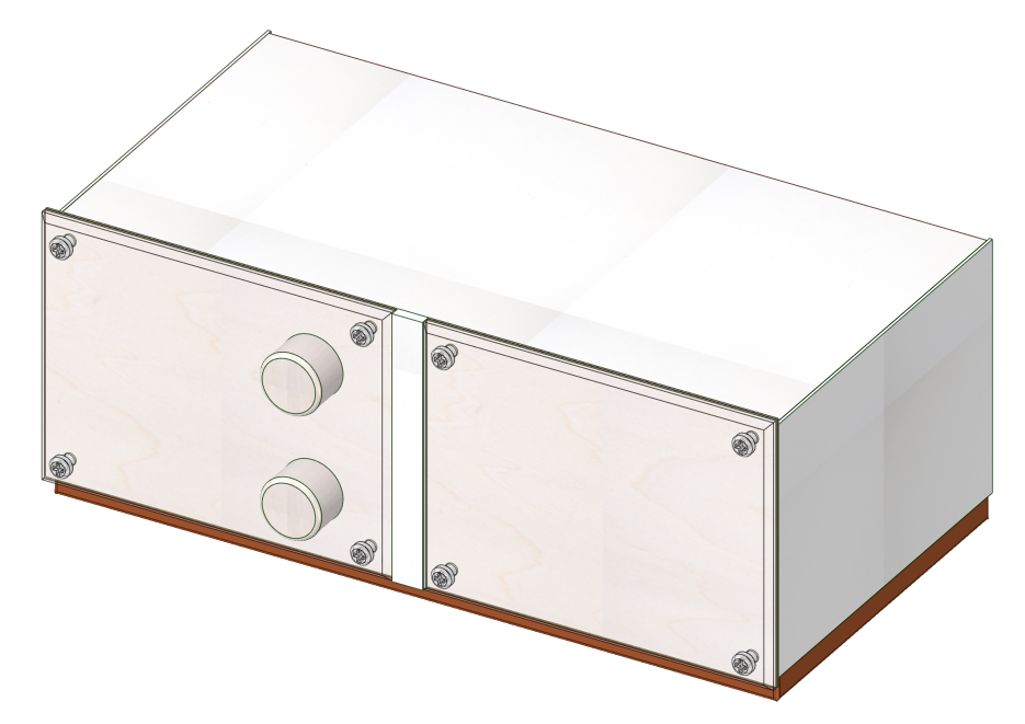
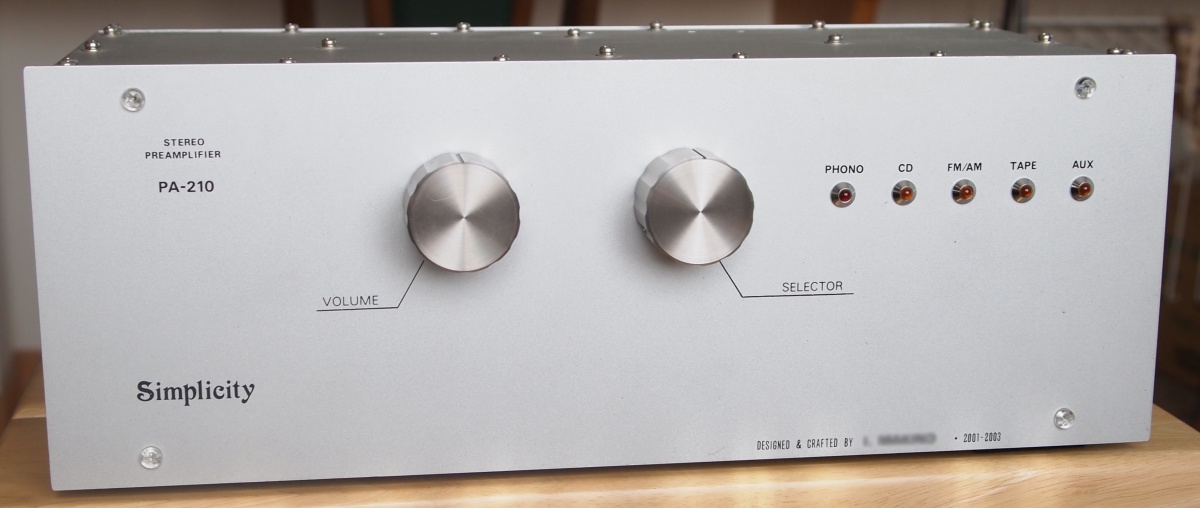
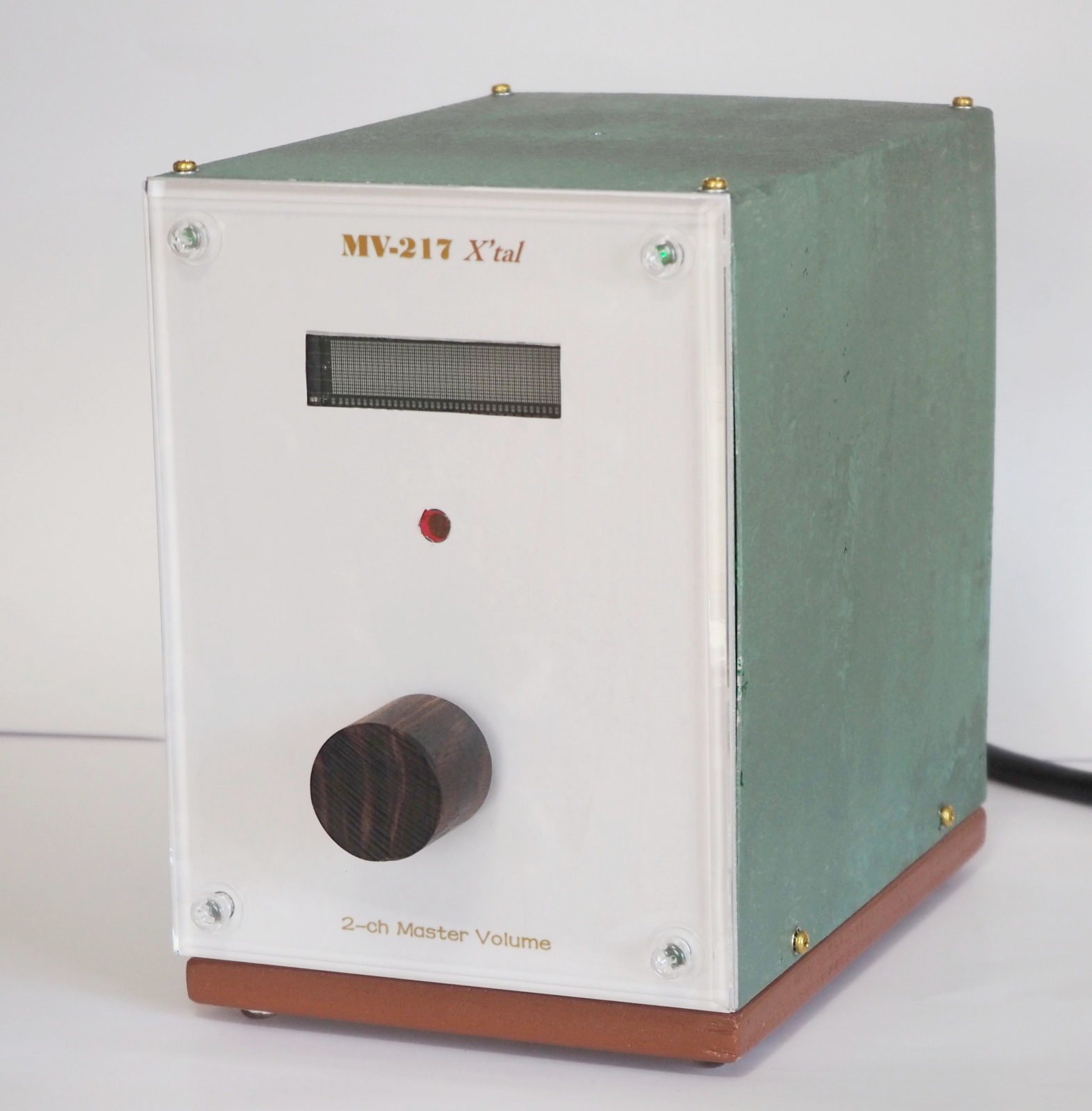
The design combines elements from two of my past works: PA-210 Simplicity and MV-217 X'tal. It reflects my personal taste while also offering a familiar and intuitive user experience.
| PA-210 Simplicity | MV-217 X'tal |
 |
 |
Design of Front Panel
The components used on the front panel are the same as those on the MV-217.
It’s essentially MV-217’s layout turned sideways, with two units placed
side by side.
By removing the clear plastic screws, you can detach the front panel.
These clear screws also function as power indicators.
As with the MV-217, the knobs are made of wood. To achieve a lighter tone,
I chose cherry wood.
Three 7-segment LEDs are used for the numeric display. I initially intended
to use orange LEDs.
For the selector indicators, a red LED is used for PHONO, and orange LEDs
are used for DAC and AUX. This follows the design of the indicators on
the PA-210.
A key point is to make the LEDs invisible when they are turned off.
To check the appearance, I conducted a preliminary experiment. I applied
stickers to ROHM’s orange 7-segment LED and turned them on.
To my surprise, I found that light leaked into adjacent segments. In the
photo below, the brightness difference between a lit segment and its adjacent
unlit segment looks clear, but to the naked eye, the difference is barely
noticeable. For example, when displaying '0', it looks more like an '8'.
This is unacceptable. I never expected ROHM to ship such low-quality products.
Since I couldn’t find any orange 7-segment LEDs available for purchase
in single units, I reluctantly selected a plain red LED. I’m not fond of
red LEDs because they are too harsh on the eyes, though.
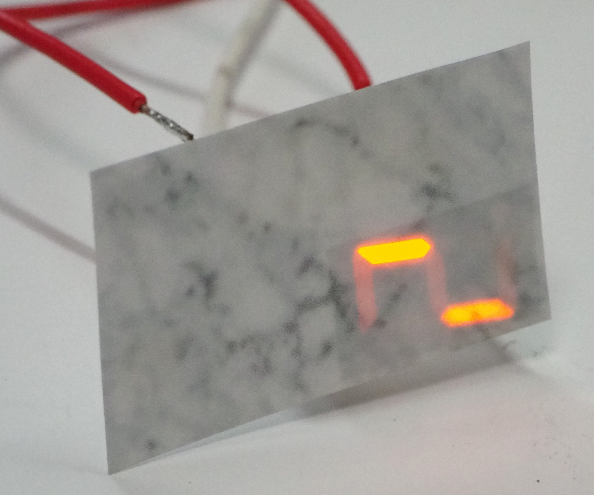 |
| Experiment using ROHM LA-601, 7-seg LED Light leaks into adjacent segments. To the naked eye, the lit segments look a little darker. |
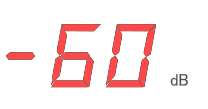
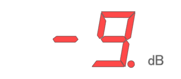
The numeric display can show values from -99 through +99, but in actual
use, it displays gain values from -95.5 through +10.
A gain of -∞ dB is represented by just a single '-'. A 0.5 dB increment
is indicated by a decimal point only.
 |
 |
 |
 |
| -∞dB (mute) No numeric character is displayed |
-60dB |
-9.5dB The upper digit's '0' is suppressed The decimal point indicates '0.5dB' |
+3dB '+' is not displayed (can't be) |
| Mismatch Sign |
 |
| It indicates that the angle of VOL knob doesn't match the actual gain |
The Front Panel Display operates in one of the four modes:
- Quick
- Display turns on only when the user changes the gain or the source.
Display turns off after three seconds elapse, if the user turned the knob.
Display indicates 'Mismatch Sign' after three seconds elapse, if the user used the remote.
This is the default mode. - Permanent
- Display is always on.
- Analog
- Display does not turn on when the user turns the knob, while Display turns
on for three seconds when the user uses the remote.
CC-218 looks like a pure analog amplifier unless the user uses the remote. This is why I named it 'Analog' mode.
If the user uses the remote, Display indicates 'Mismtach Sign' three seconds later.
- Disable
- Display is always off.
Construction
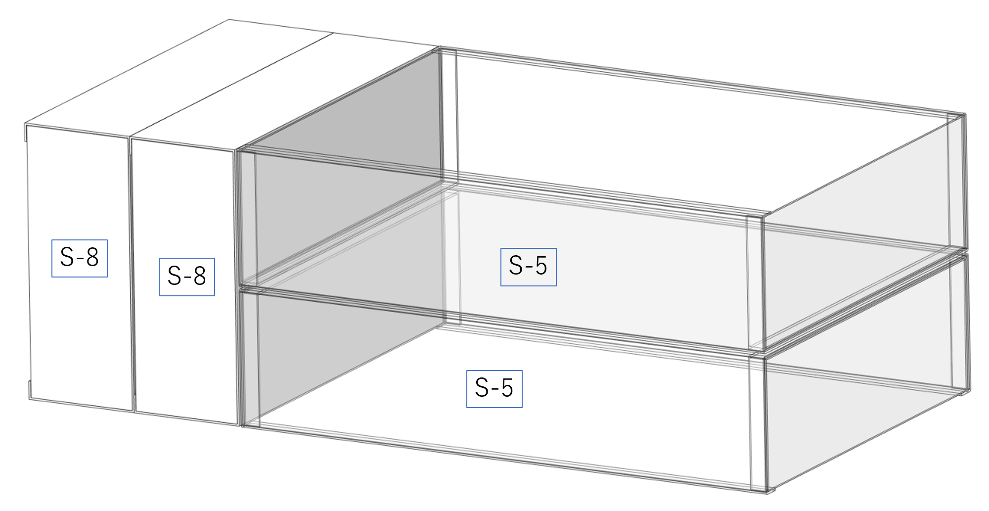
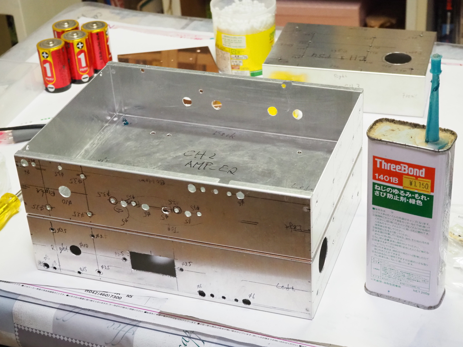
At this stage, I decided to use commercially available chassis to construct the case: two units of LEAD S-5 and two units of LEAD S-8. The S-5 will be used for the clean compartment, and the S-8 for the dirty compartment.
Clean compartment – houses the analog circuitry
Dirty compartment – houses the digital circuitry and power supply unit
At this stage, the plan was to install L-ch (the left channel) circuitry in the upper S-5 unit and R-ch (the right channel) in the lower one—this is the so-called dual-mono construction, the same structure used in the PA-202, PA-203, and PA-210.
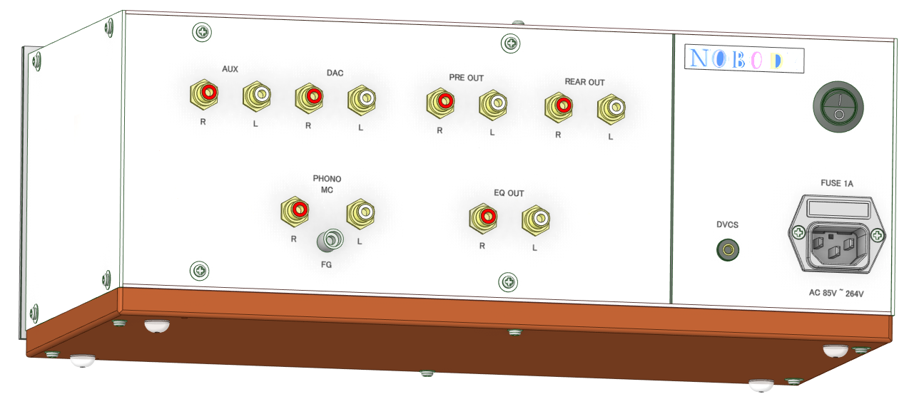
Design of Back Panel
On the back side, an aluminum panel with a sticker on it will be mounted.
The PHONO input supported both MM and MC cartridges at this stage, though,
it was later revised to support MC only.
Design of the other out panels
Top Panel and Side Panels will be painted using automotive spray paint. The color will be silver metallic.
A 12mm-thick MDF board will be attached to Bottom Panel. This is intended to lower the center of gravity of the case and give it a more stable appearance, while also providing the added benefit of suppressing vibrations. The MDF board will be painted brown.
Mechanical Design
The “bar nut” that I devised during the design of the PA-210 has been adopted once again. It’s a mechanical part made by drilling a threaded hole into an aluminum square bar, allowing it to function as a nut. The term “bar nut” is a word I coined myself. It is used to fasten the chassis and panels together.
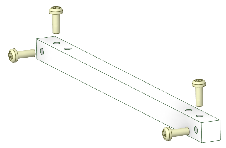 |
 |
| Bar nut | Fastening chassis and panels together |
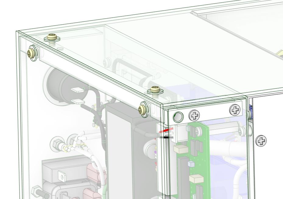
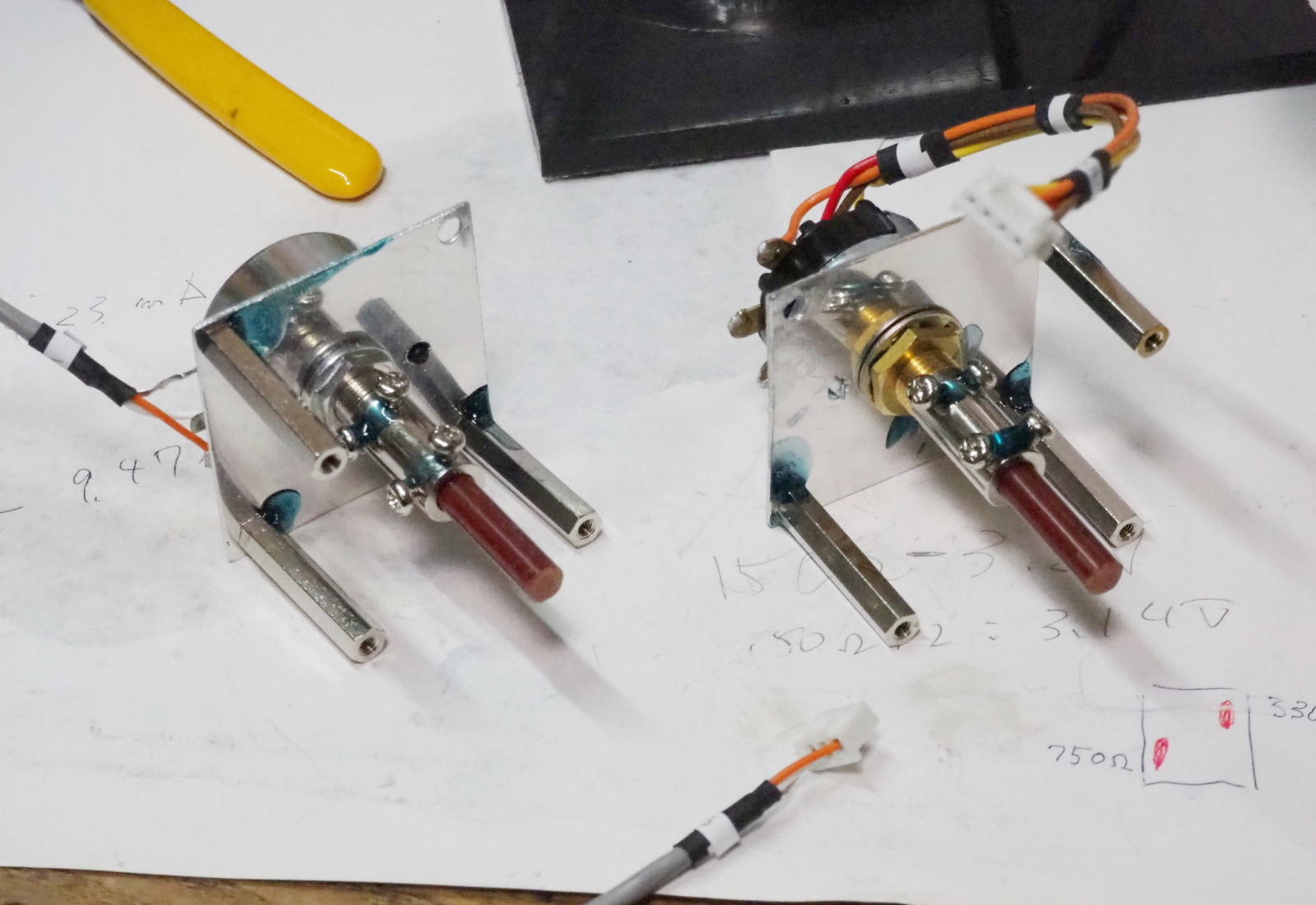
The VR and the rotary switch for input selection are mounted using a subpanel, just like in the MV-217. The VR is positioned slightly behind the front panel, and an extension shaft is attached to it. By adjusting the length of the extension shaft, the position of the knob is precisely aligned. The gap between the knob and the transparent panel is adjusted to be approximately 1 mm.
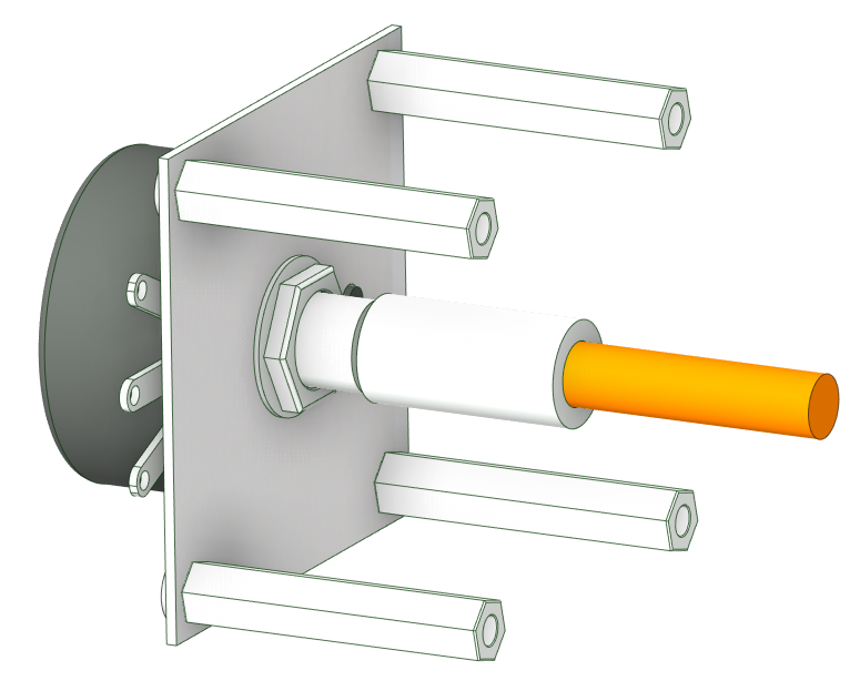 |
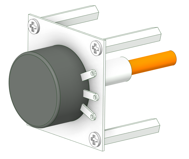 |
| VR Module (front) | VR Module (back) |
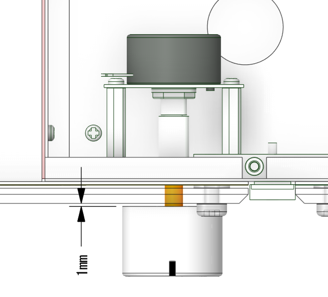 |
| Mounting VR Module - Top view |
A 1mm-thick copper plate was placed between the upper and lower clean compartments.
Another 1mm-thick copper plate was also inserted between the clean compartment
and the dirty compartment.
This was done to achieve both electromagnetic shielding and vibration damping
effects.
As a result of the mechanical design, the appearance turned out as shown
in the illustration below.
Please note that this is not the final design. Since the mechanical design was done in the early stage of the development
process, some changes were made in later stages. The reason for presenting
this interim design is to share some of the design know-how with readers.
 |
| Appearance after mechanical design - Front |
For more details on the mechanical design, please refer to the mechanical
design document below. Since this is not the final stage of the design,
dimensions are not included.
This document also does not cover the design of the panels, as changes
may occur during Layout and Wiring Design phase.
<Mechanical design document:CC-218_Design_Mech.pdf>
Layout and Wiring Design
In this design phase, there are the following three steps:
- Module layout
- Materialize the rough image of module configuration made during the stages of appearance design and mechanical design into concrete forms such as block diagram, and determine the arrangement of the circuit boards and the AC/DC converters inside the case.
- Definition of PCB specification
- Determine dimensions of PCBs, select connectors, and determine the positions of the connectors in the PCBs.
- Wiring design
- Design wire harnesses used for internal connections.
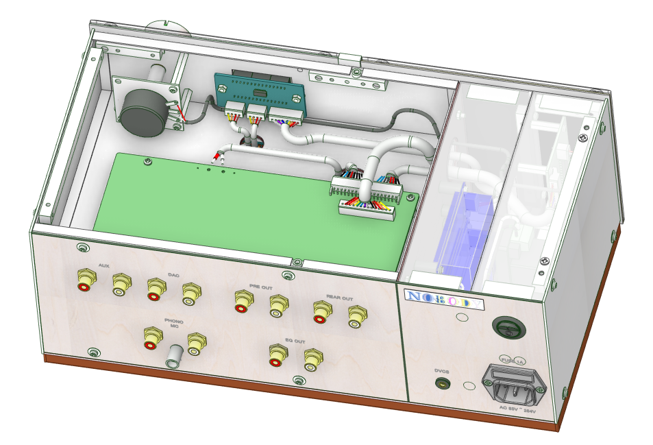
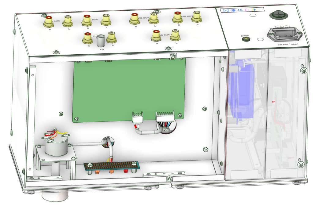
Module layout
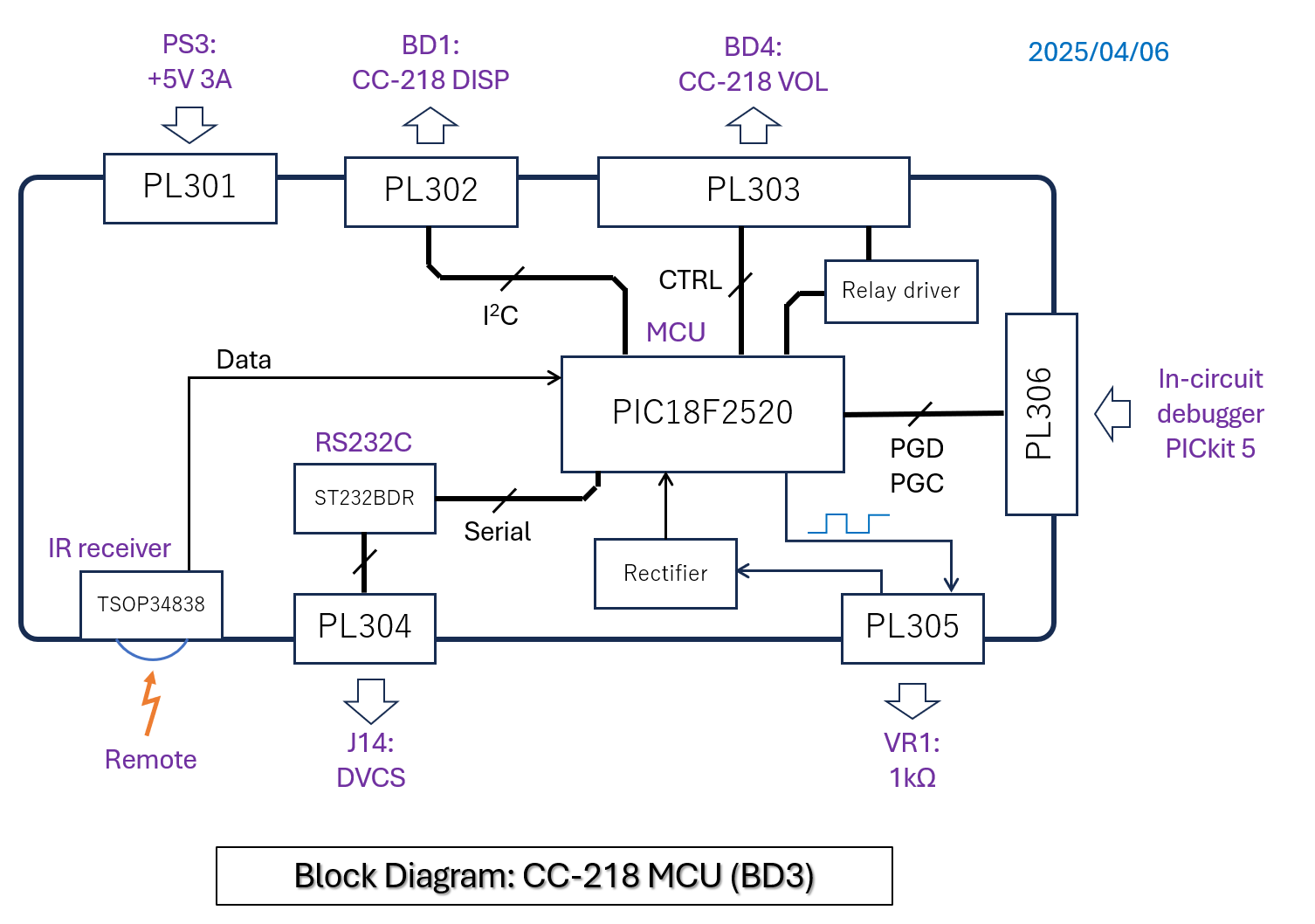
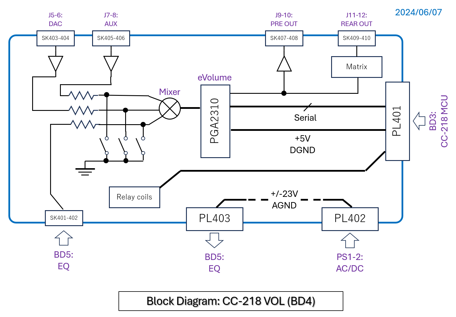
The figure below shows the block diagram of CC-218.
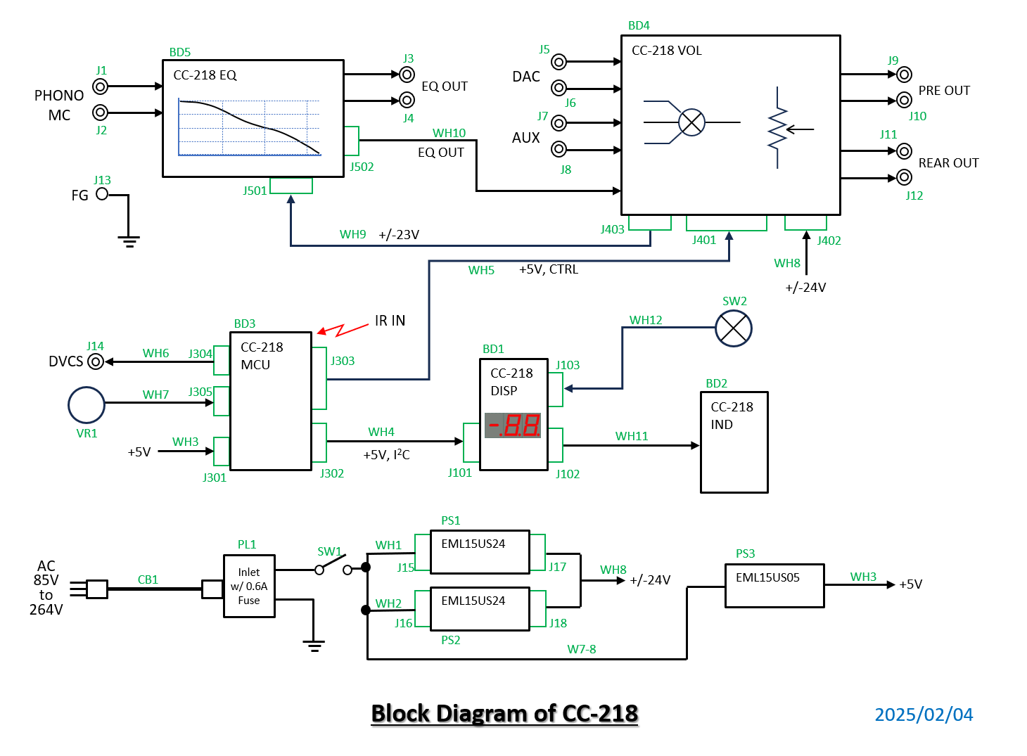
The table below describes each module and shows the arrangement.
| Reference designator | Module | Feature | Location |
|---|---|---|---|
| PL1 | AC inlet | AC inlet (IEC 60320 C14) w/ fuse holder | Back Panel |
| PS1 | AC/DC converter (UML15US24-T) |
Power supply unit for analog circuits +24V 0.6A |
CH3 PSU (Dirty compartment for PSU) |
| PS2 | AC/DC converter (UML15US24-T) |
Power supply unit for analog circuits -24V 0.6A |
CH3 PSU (Dirty compartment for PSU) |
| PS3 | AC/DC converter (UML15US05-S) |
Power supply unit for digital circuits 5V 3A |
CH4 MCU (Dirty compartment for MCU) |
| BD1 | CC-218 DISP | 2.5-digit 7-seg LED Display Controlled by AS1115 |
CH1 AMP_VOL (Clean compartment) |
| BD2 | CC-218 IND | Selector Indicator Using 3 LEDs |
CH2 AMP_EQ (Clean compartment) |
| BD3 | CC-218 MCU | Controller Board MCU: PIC18F2520 |
CH4 MCU (Dirty compartment for MCU) |
| BD4 | CC-218 VOL | Volume Board Using PGA2310 |
CH1 AMP_VOL (Clean compartment) |
| BD5 | CC-218 EQ | Phono EQ Board Using LT1115 |
CH2 AMP_EQ (Clean compartment) |
Considering the layout, I realized that a dual-mono construction not only
fails to improve sound quality, but can actually degrade it. This is because
separating the ground (GND) for the left and right channels can create
ground loops and lead to unnecessary internal wiring. While the term “dual-mono
construction” sounds impressive, it is a structure with little real benefit.
I almost adopted it out of habit, since it was used in the PA-202, PA-203,
and PA-210, but ultimately decided against it.
In addition, sufficient channel separation can be achieved even with an
ordinary constuction.
I revised the mechanical design to place the volume board (BD4) in the
upper clean compartment and the phono EQ board (BD5) in the lower compartment.
Accordingly, the exterior appearance was changed.
Other modifications include making the PHONO input exclusive to MC cartridges
and replacing the AC inlet with one that has a built-in fuse holder, among
a few other changes.
 |
 |
| Front | Back |
Specifications of boards
PCBs are used for BD1 and BD3 through BD5.
Each PCB is assigned the same number as its corresponding board's reference
designator. There is no PCB2; that number is unused.
| Reference designator | Module | Bare board | Specification |
|---|---|---|---|
| BD1 | CC-218 DISP | PCB1 Manufactured by maker |
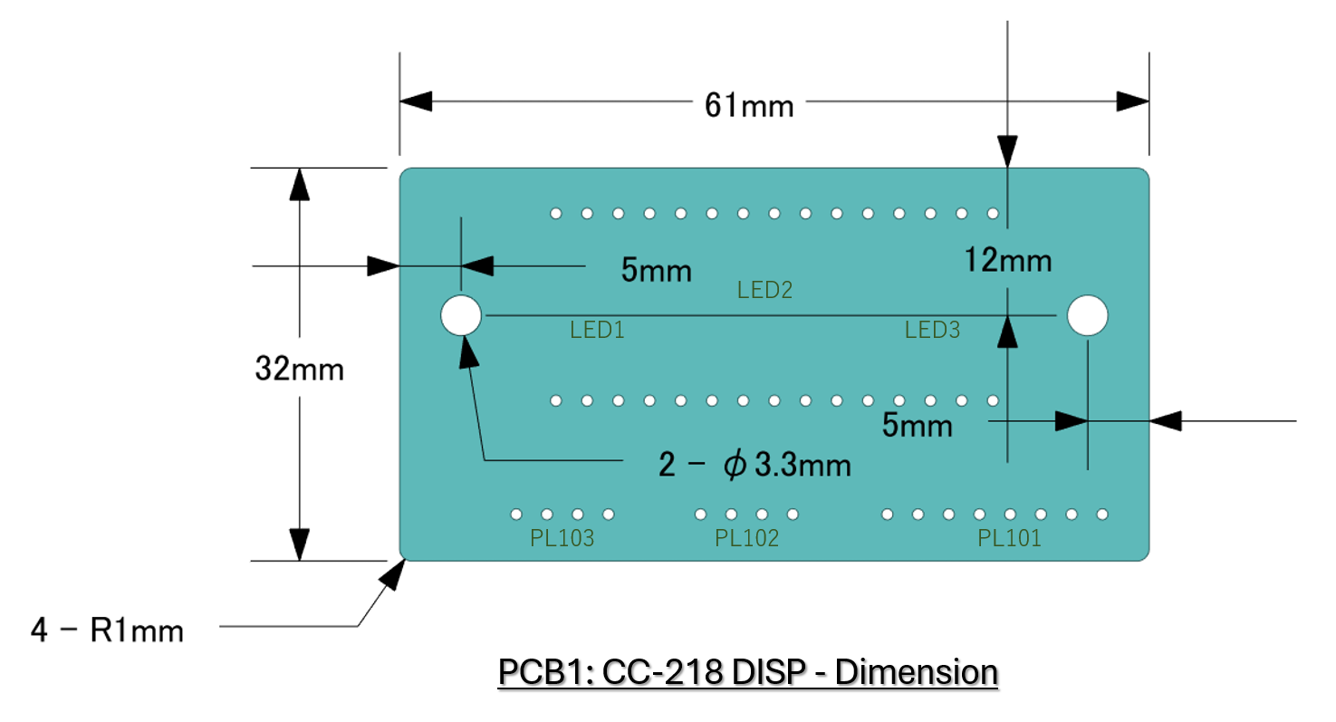
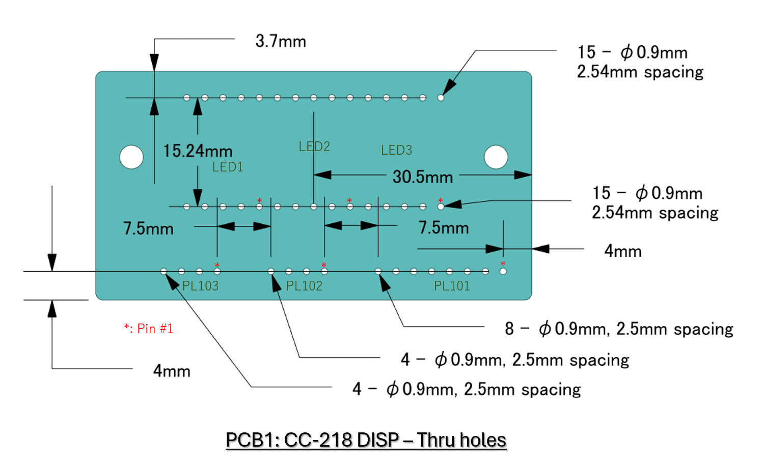
Double-sided thru hole PCB 1.6 x 61 x 32mm |
| BD2 | CC-218 IND | Selector Indicator Using 3 LEDs |
Single-sided universal board 1.6 x 68 x 20mm |
| BD3 | CC-218 MCU | PCB3 Manufactured by maker |
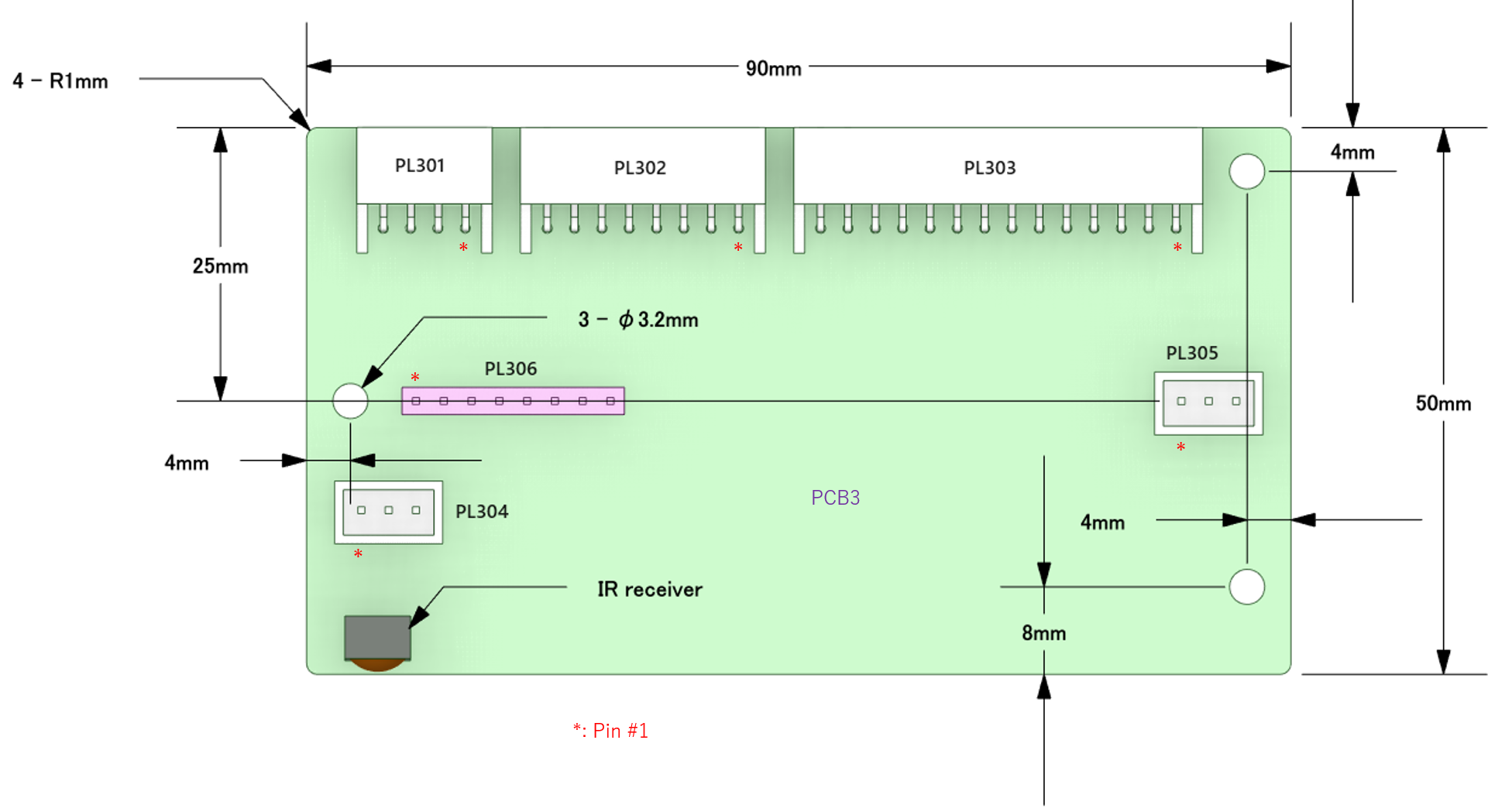
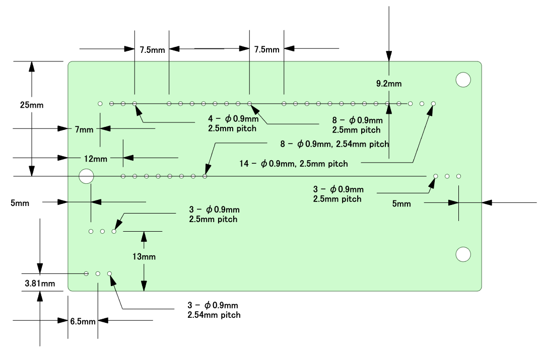
Double-sided thru hole PCB 1.6 x 90 x 50mm |
| BD4 | CC-218 VOL | PCB4 Manufactured by maker |
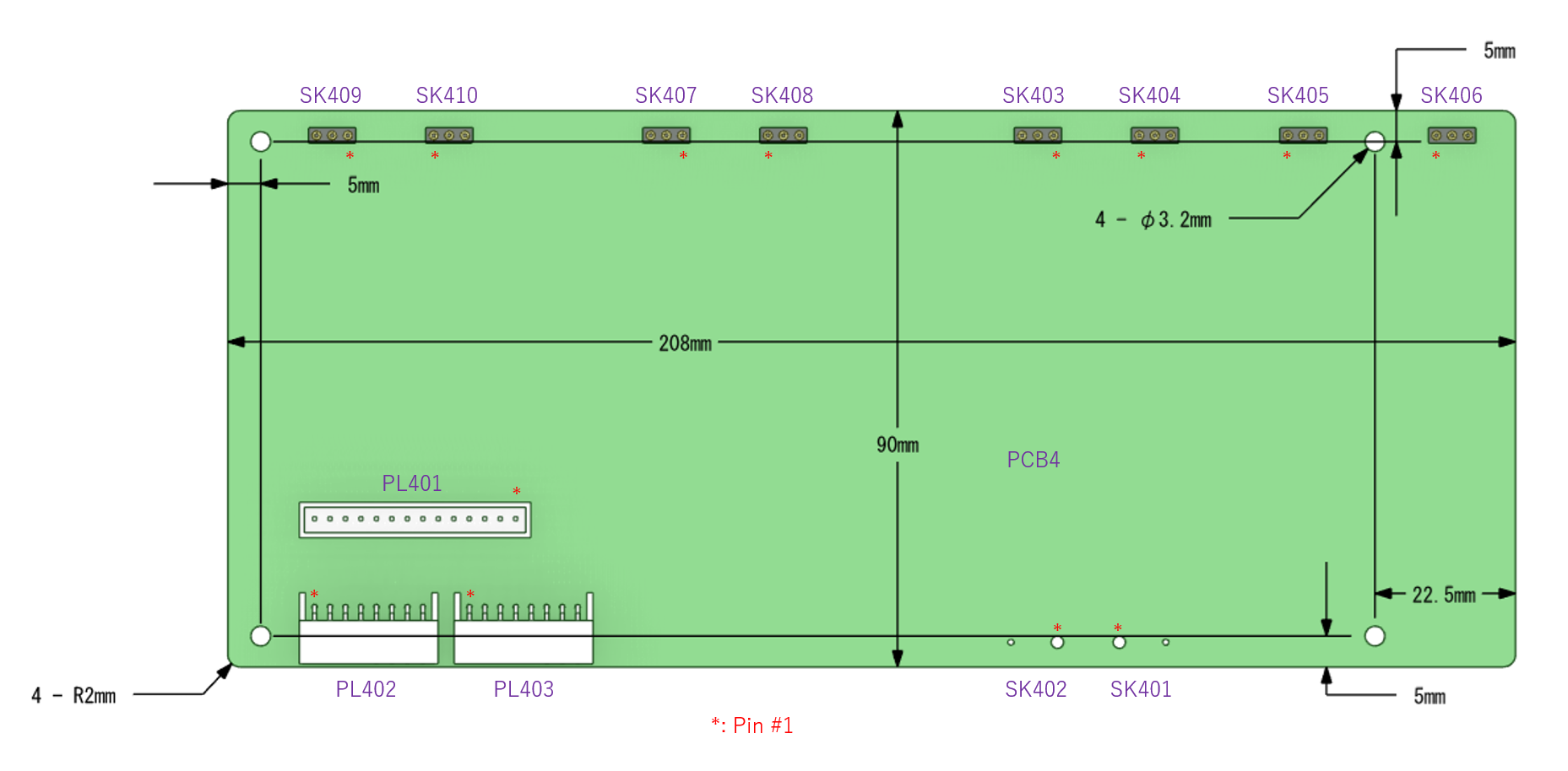
Double-sided thru hole PCB 1.6 x 208 x 90mm |
| BD5 | CC-218 EQ | PCB5 Manufactured by maker |
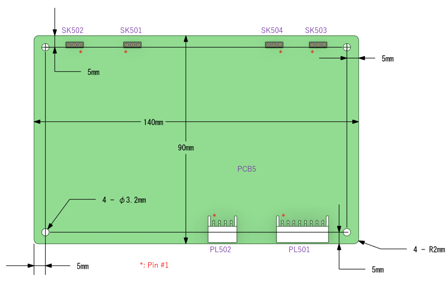
Double-sided thru hole PCB 1.6 x 140 x 90mm |
All the connectors used for internal connections are JST (Japan Solderless
Terminal) XH series connectors. These were also used in the MV-217, so
I already have the tool and am familiar with their use.
Connections between Back Panel connectors and the PCBs will be made using
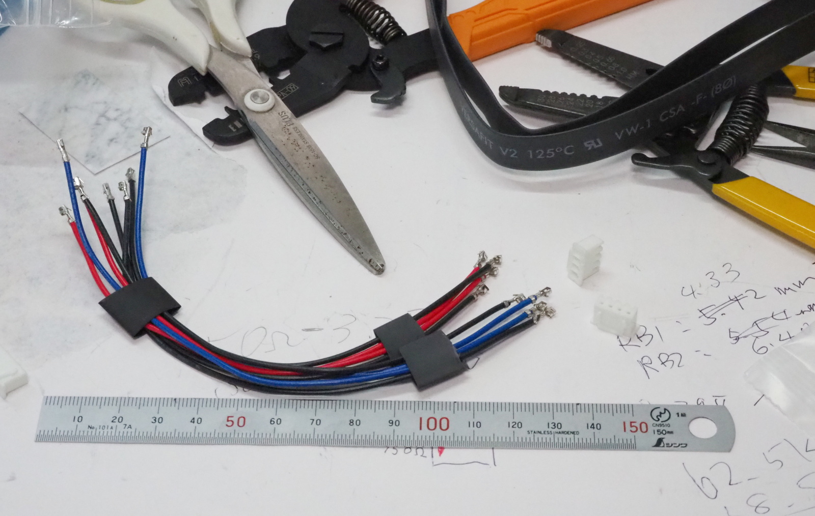
either 0.5mm gold-plated OFC wire or 1/4W resistors. The connector side
will be soldered, while the PCB side will be connected via pin sockets.
 |
 |
| CC-218 DISP Dimension |
CC-218 DISP Thru holes for connectors and 7-seg LEDs |
 |
 |
| CC-218 MCU Dimension |
CC-218 MCU Thru holes for connectors and IR receiver |
 |
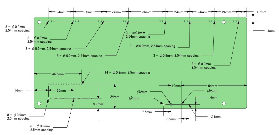 |
| CC-218 VOL Dimension |
CC-218 VOL Thru holes for connectors and pin sockets |
 |
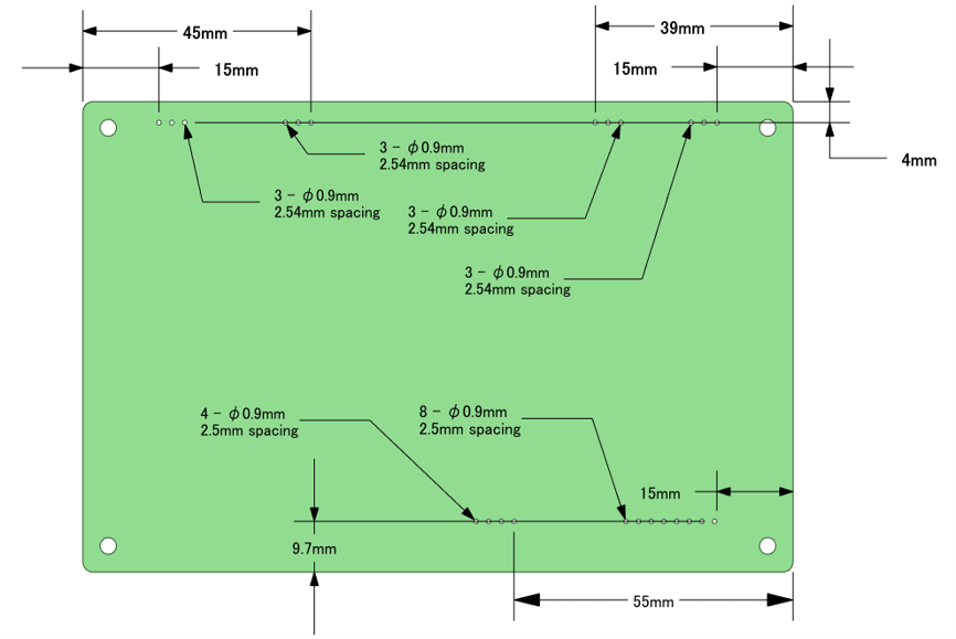 |
| CC-218 EQ Dimension |
CC-218 EQ Thru holes for connectors and pin sockets |
Wiring design
The table below shows the wires used on CC-218.
| Use | Type/spec | Gauge | Color |
|---|---|---|---|
| Power supply Primary |
UL1015 Rating: 600V |
AW18 | Earth:Green, Line:Black, Neutral:White (Conforming to standard) |
| Power supply Secondary |
UL1007 Rating: 300V |
AW22 | GND:Black, Positive supply:Red, Negative supply:Blue |
| Board to board Digital |
UL1007 Rating: 300V |
AW22 | P1: Brown, P2: Red, ... (The color corresponds to pin number of connector) |
| Board to panel Digital |
Canare L-2B2AT Dual-core coaxial |
AWG25 (core) | Grey |
| Analog | Neglex 2520 Single-core coaxial |
Sub-miniature | L-ch: white R-ch: Red |
| Board to panel Analog |
Amtrans AMOFC-GMK-05FC |
0.5mm dia. OFC |
I used mechanical CAD (DesignSpark Mechanical) to design wiring.
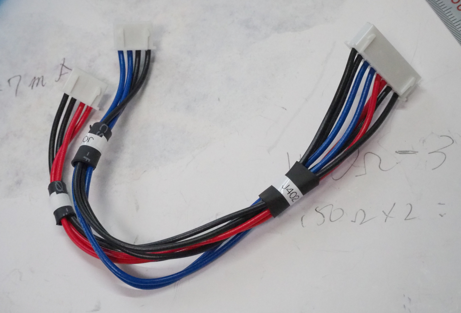
Here's an example: The CAD shows routing of the wire harness (WH5 VOL_SEL)
and its length.
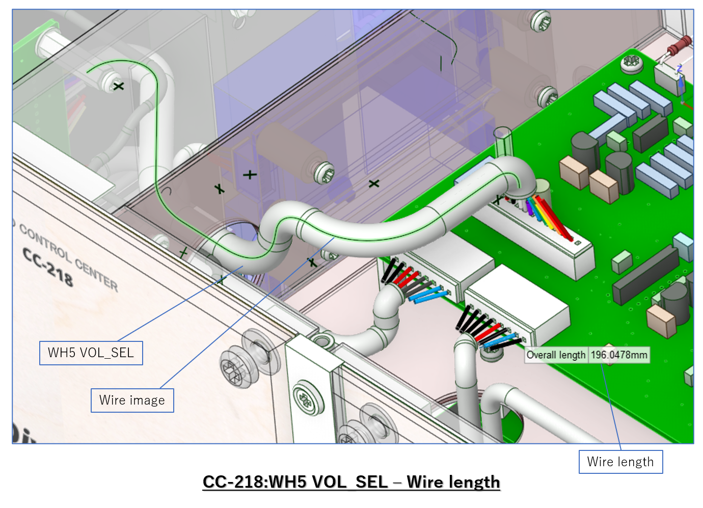
In the above example, CAD calculates the wire length and the result is
196mm. Some margin has to be added to this length to connect the wire to
the connector.
I added 40mm and the total length becomes 236mm in case of WH5.
The way of connecting the boards to the RCA jacks in Back Panel is one of the unique idea employed in CC-218; using 0.5mm gold-plated OFC wires or resistors instead of wire harnesses. One end of the wire/resistor is soldered to the RCA jack while the other end is inserted into the pin socket on the board.
For further details of layout and wiring, see the following PDFs.
<Design document of layout and wiring: CC-218_Design_LayoutWiring.pdf>
<Wire harness assembly manual: CC-218_Design_WireAssy.pdf>
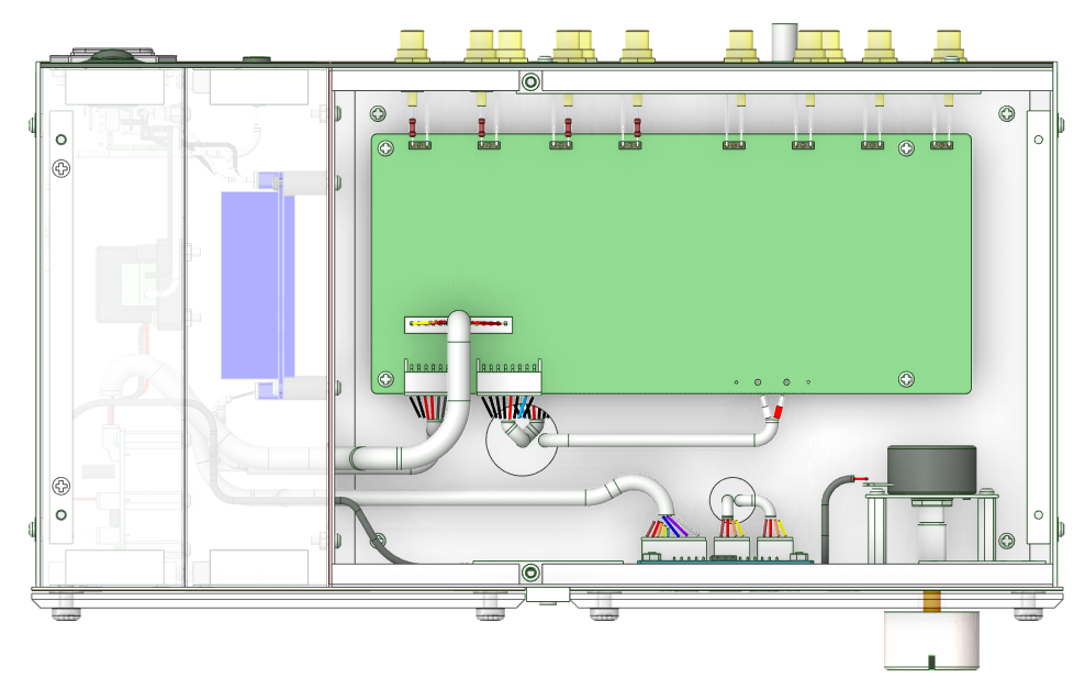 |
 |
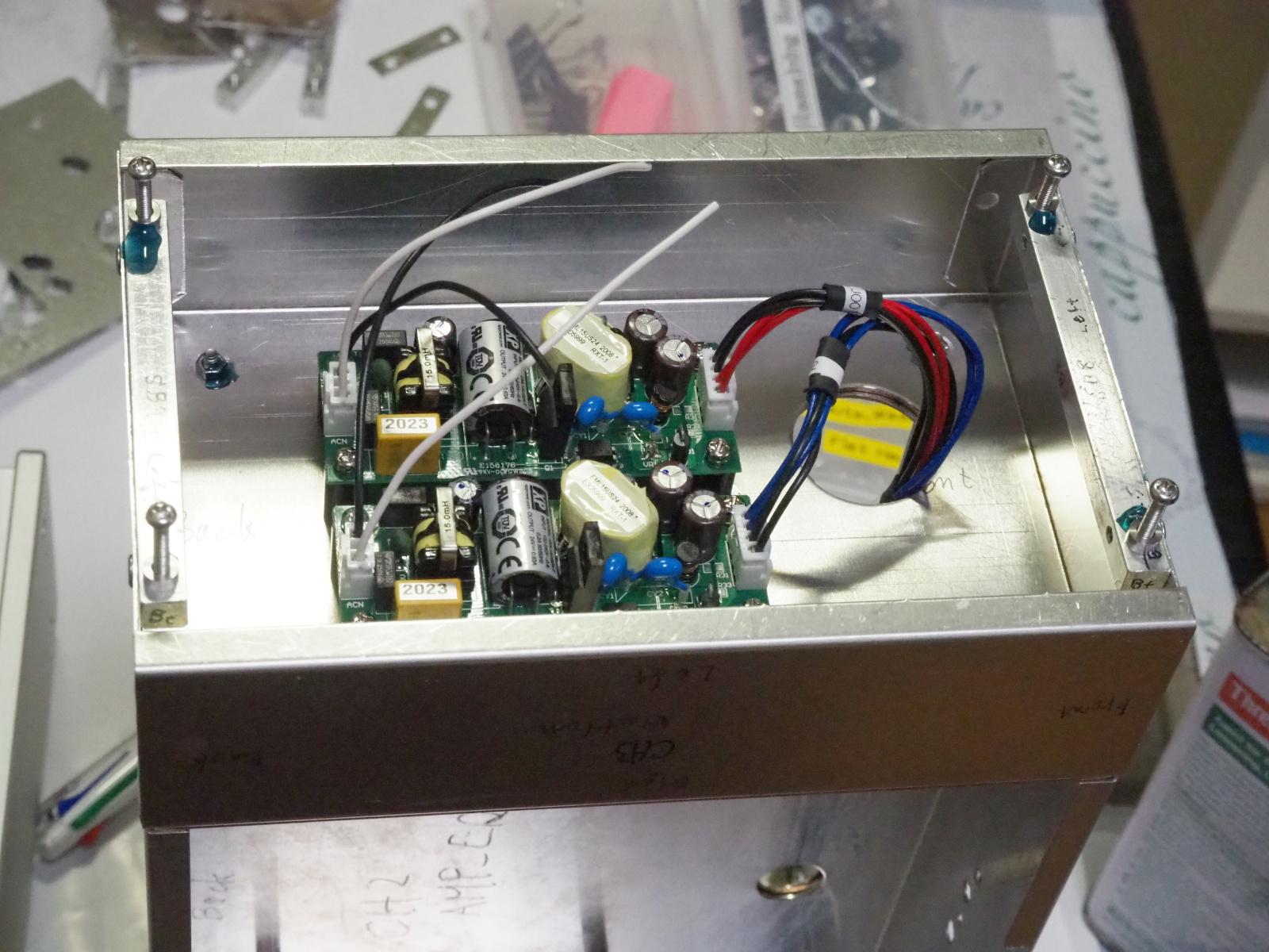
| Upper clean compartment (CH1 AMP_VOL) |
Upper clean compartment (CH1 AMP_VOL) |
 |
 |
| Lower clean compartment (CH2 AMP_EQ) |
Dirty compartment (CH4 MCU) Thru holes for connectors and IR receiver |
 |
 |
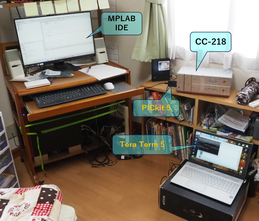
| Connection of ICD Remove Side Panel L (PN6), and insert ICD (PICkit 5) to pin header (BD3:PL306) on Controller Board (BD3 CC-218 MCU) |
Position of IR receiver IR receiver is placed near the window of Front Panel L |
Design of outer panels
Now that the layout and wiring design is done, the design of the out panels should be fixed.
Front Panels
Here are figures of outlines of Front Panels and Front Stickers. For detailed drawings, see "metalwork manual" and "finish manual".
 |
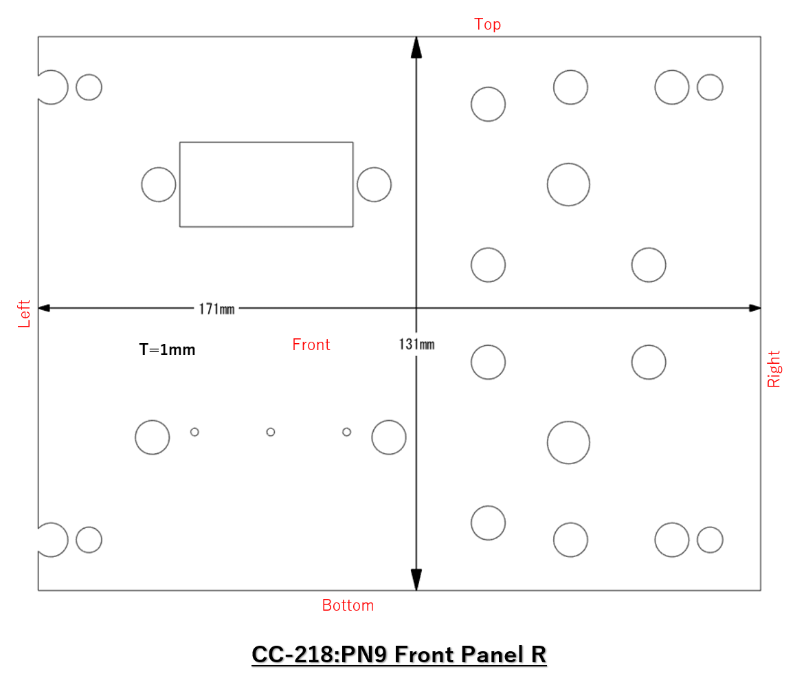 |
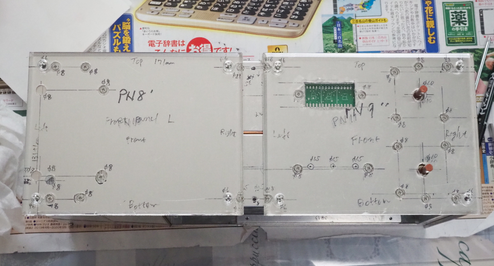
| Front Panel L (PN8) 1mm-thick aluminum panel |
Front Panel R (PN9) 1mm-thick aluminum panel |
 |
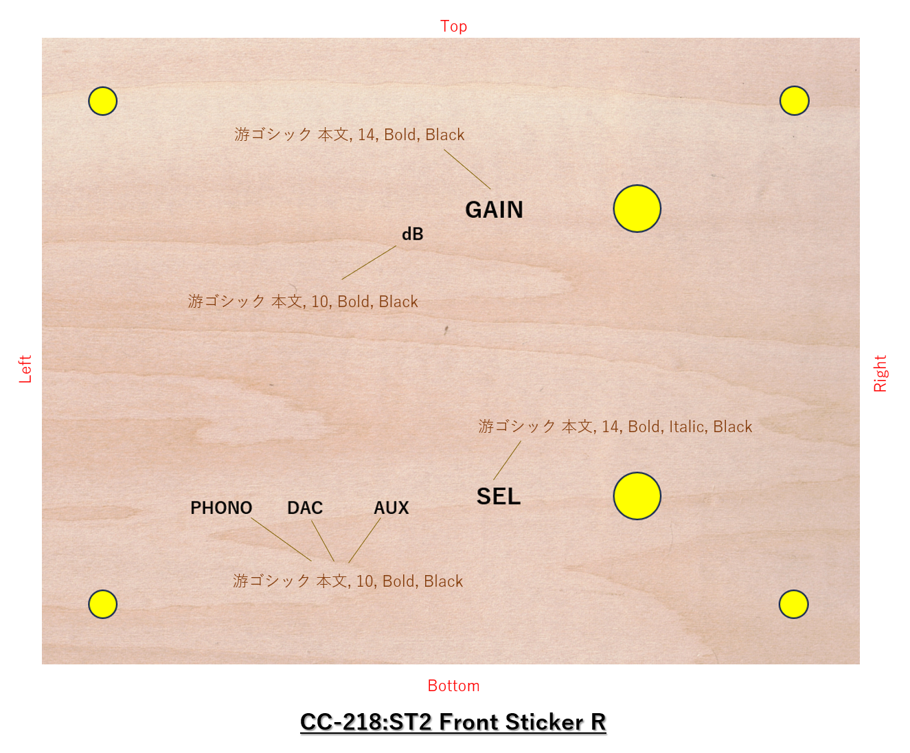 |
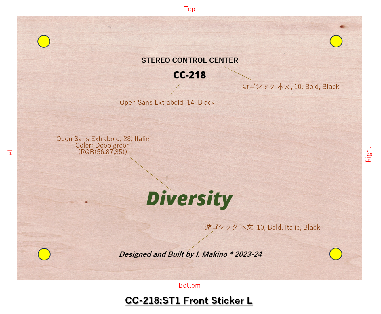
| Front Sticker L (ST1) A-one 28874N |
Front Sticker R (ST2) A-one 28874N |
Back Panels
Here are figures of outlines of Back Panels and Back Stickers. For detailed drawings, see "metalwork manual" and "finish manual".
 |
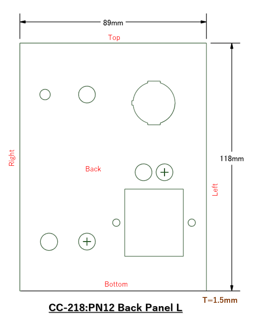 |
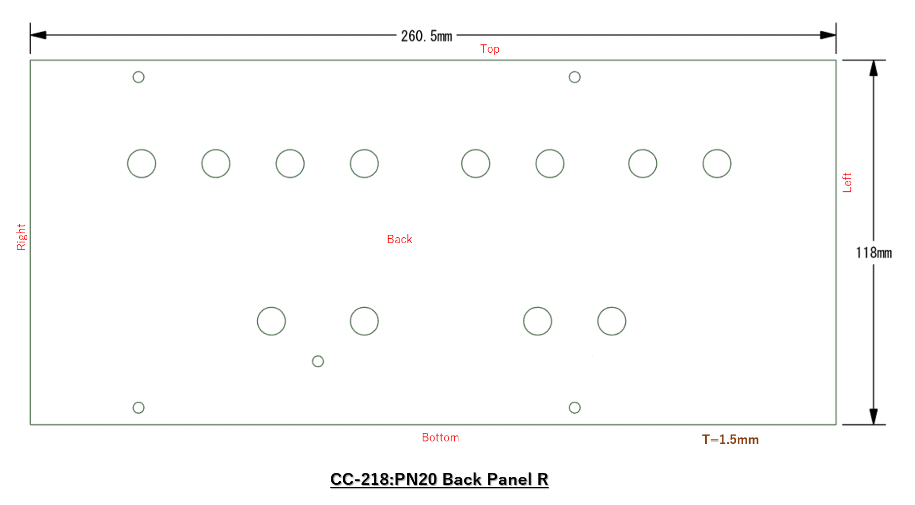
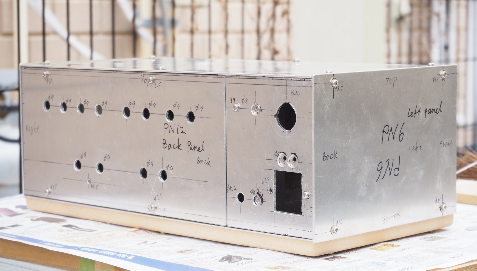
| Back Panel R (PN20) 1.5mm-thick aluminum panel |
Back Panel L (PN12) 1.5mm-thick aluminum panel |
 |
 |
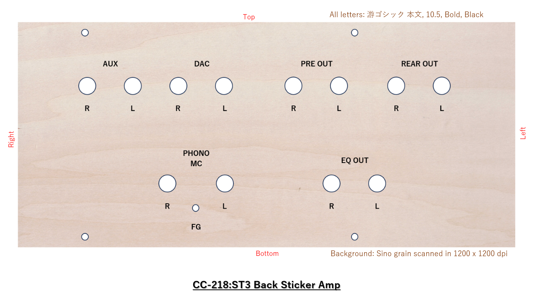
| Back Sticker Amp (ST3) A-one 28874N |
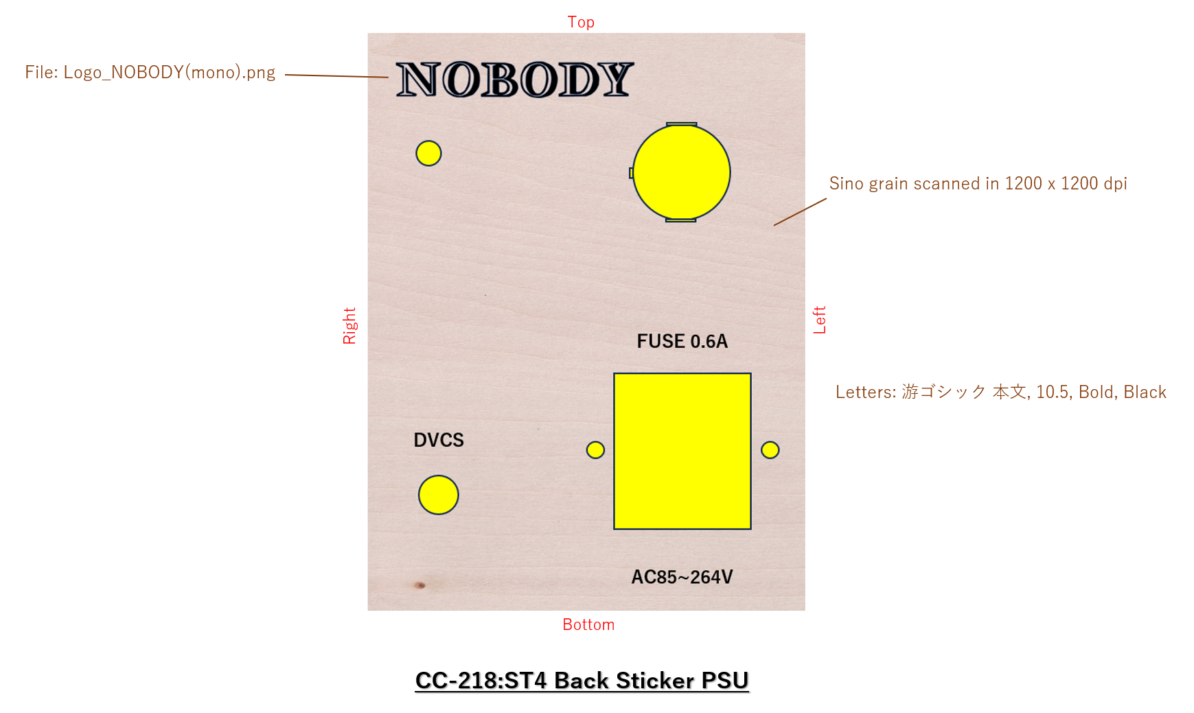
Back Sticker PSU (ST4) A-one 28874N |
Top Panel
Here are figures of outlines of Top Panel and Top Sticker. For detailed drawings, see "metalwork manual" and "finish manual".
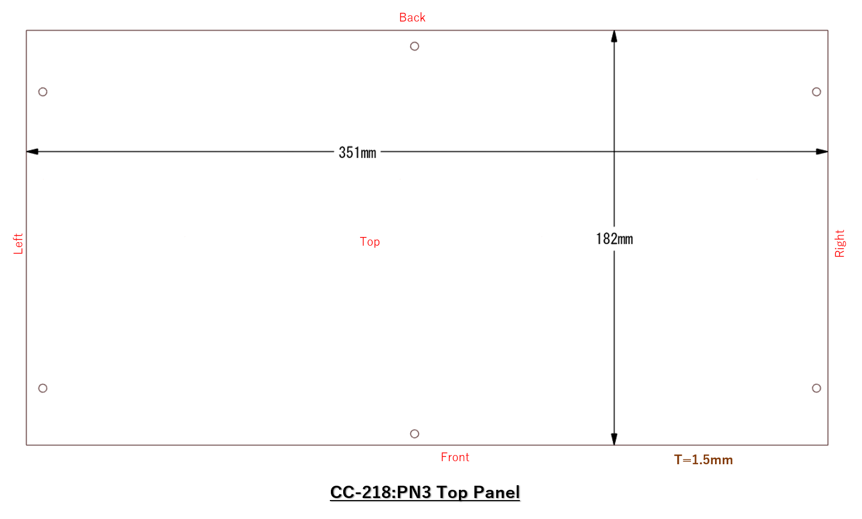 |
| Top Panel (PN3) 1.5mm-thick aluminum panel |
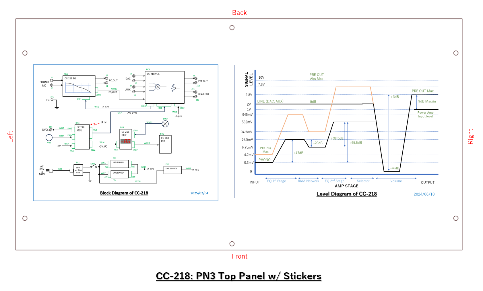 |
| Top Panel w/ Top Stickers (ST5,ST6) affixed on it ST5: Block Diagram, ST6: Level Diagram ELECOM EDT-STSC |
Drawings of Mechanical Design
Here's the metalwork manual:
<Metalwork manual: CC-218_Metalwork.pdf>
Here's the manual for processing nonmetalic materials:
<Manual for nonmetalic parts: CC-218_Woodwork.pdf>
Temporary assembly of the enclosure is necessary because the handmade mechanical
parts have dimensional errors. During the temporary assembly, each part
is to be touched up by files.
<Manual for temporary assembly: CC-218_PreAssy.pdf>
After the temporary assembly, disassemble the enclosure, and clean the
parts . After that, finish the outer panels and knobs.
<Finish manual: CC-218_Finish.pdf>
I found some bugs during creating these manuals, and revised the mechanical
design.
The purpose of the manuals is to make the labors more efficient. In addition,
creating manuals helps the desinger to find bugs because that's a kind
of simulation.
Thanks to the manuals, I could avoid unnecessary reworking in both making
parts and temporary assembly.
Circuit Design
The figure below shows the total schematic of CC-218.
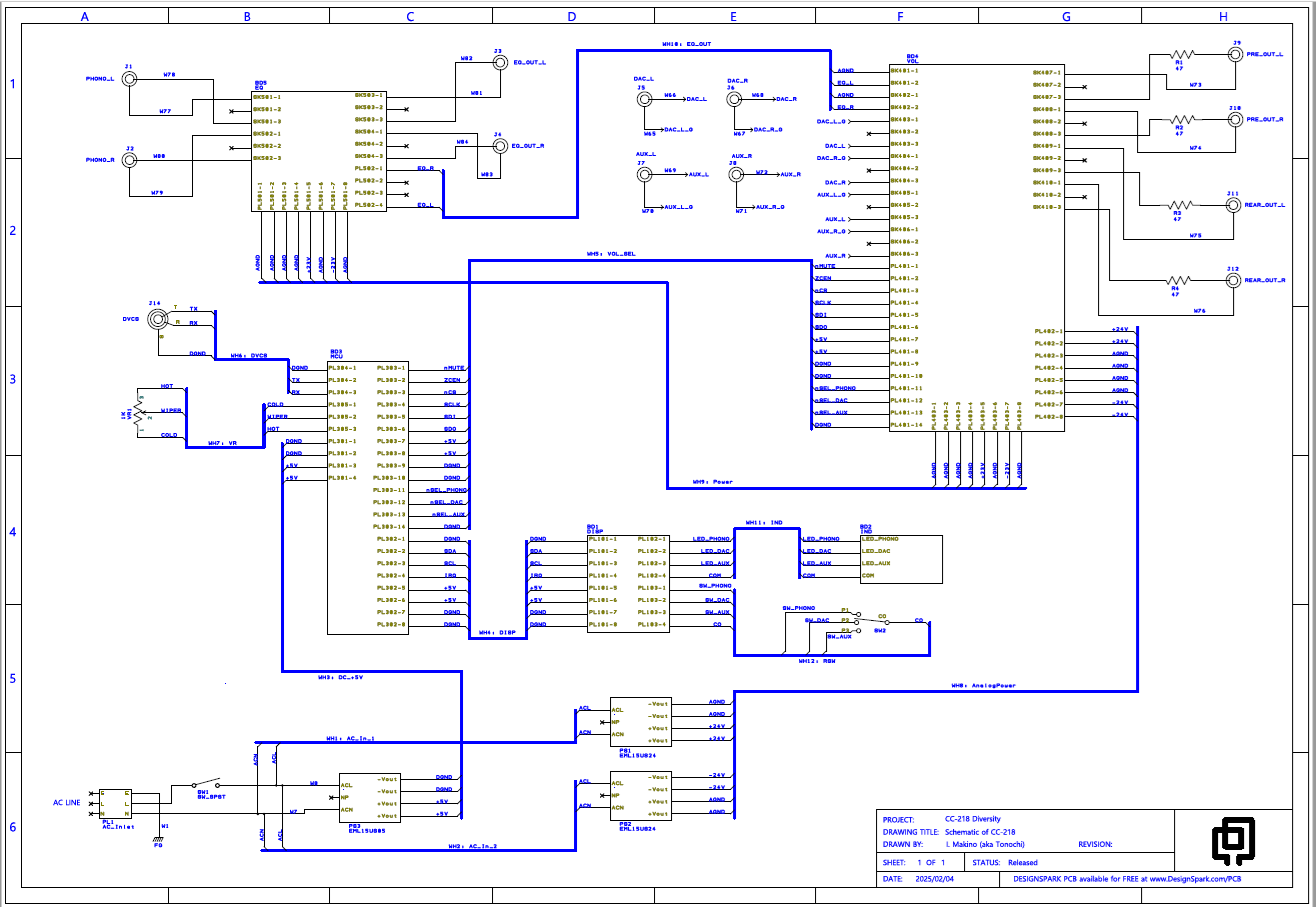
Note that the output resistors (R1~R4) are not on the board (BD4) but they are placed between the board and RCA jacks (PRE OUT, REAR OUT). The resistors are used to connect the output signals of the board to the RCA jacks instead of wire harnesses. So, the schematic of CC-218 VOL (BD4) doesn't include the output resistors.
From now on, circuit design will be carried out on board by board basis.
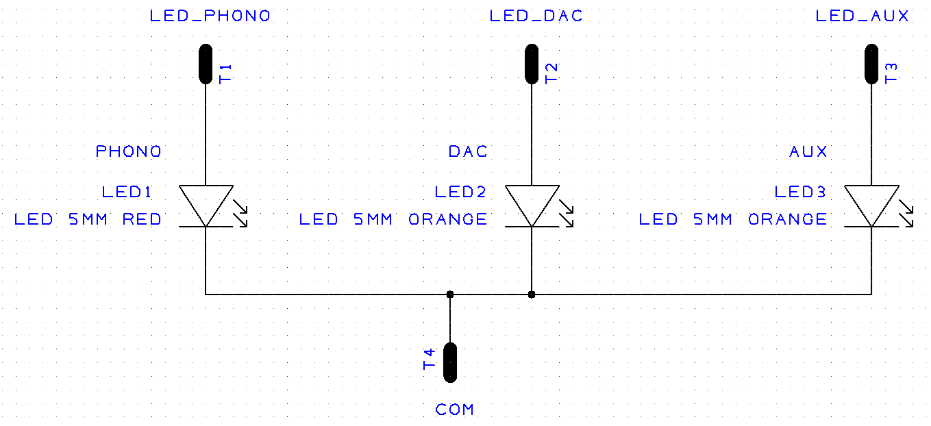
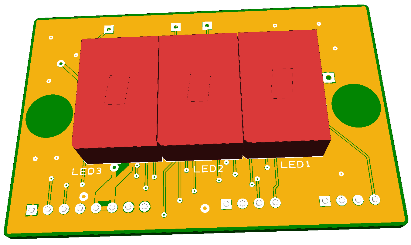
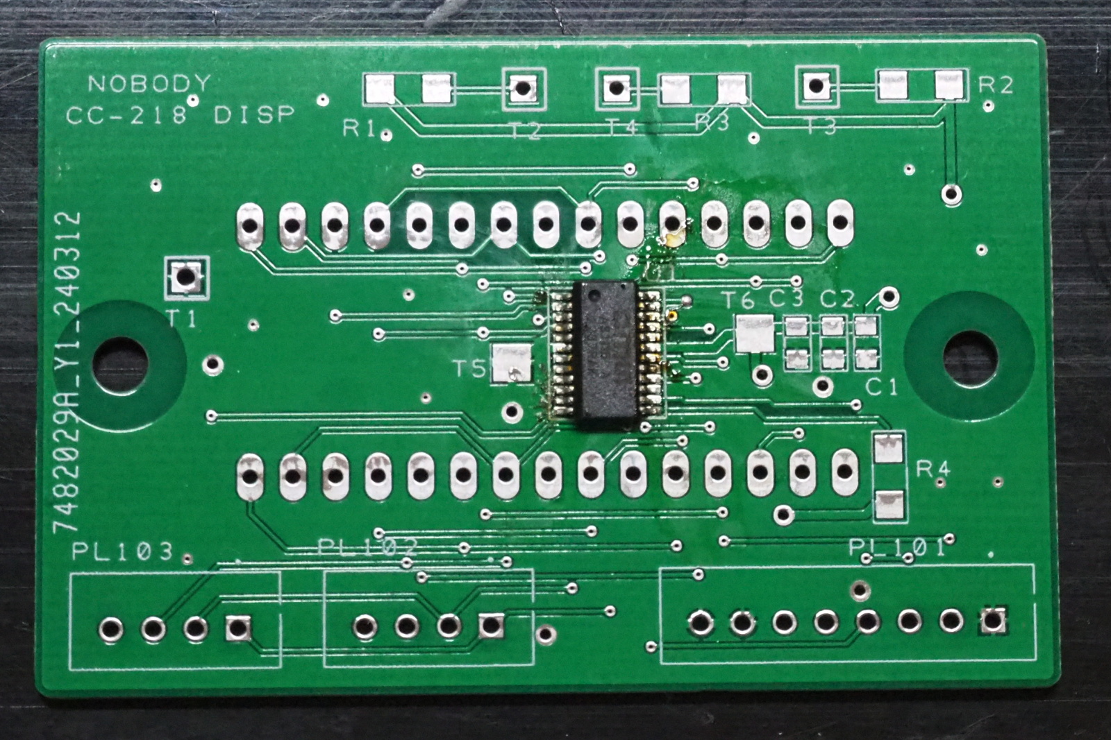
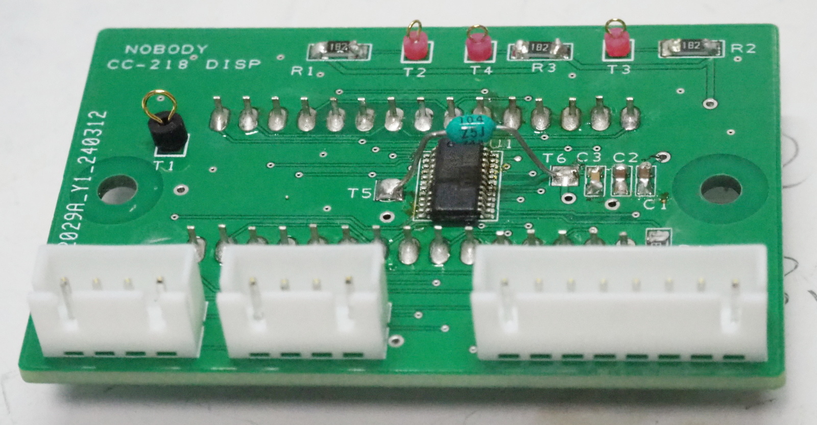
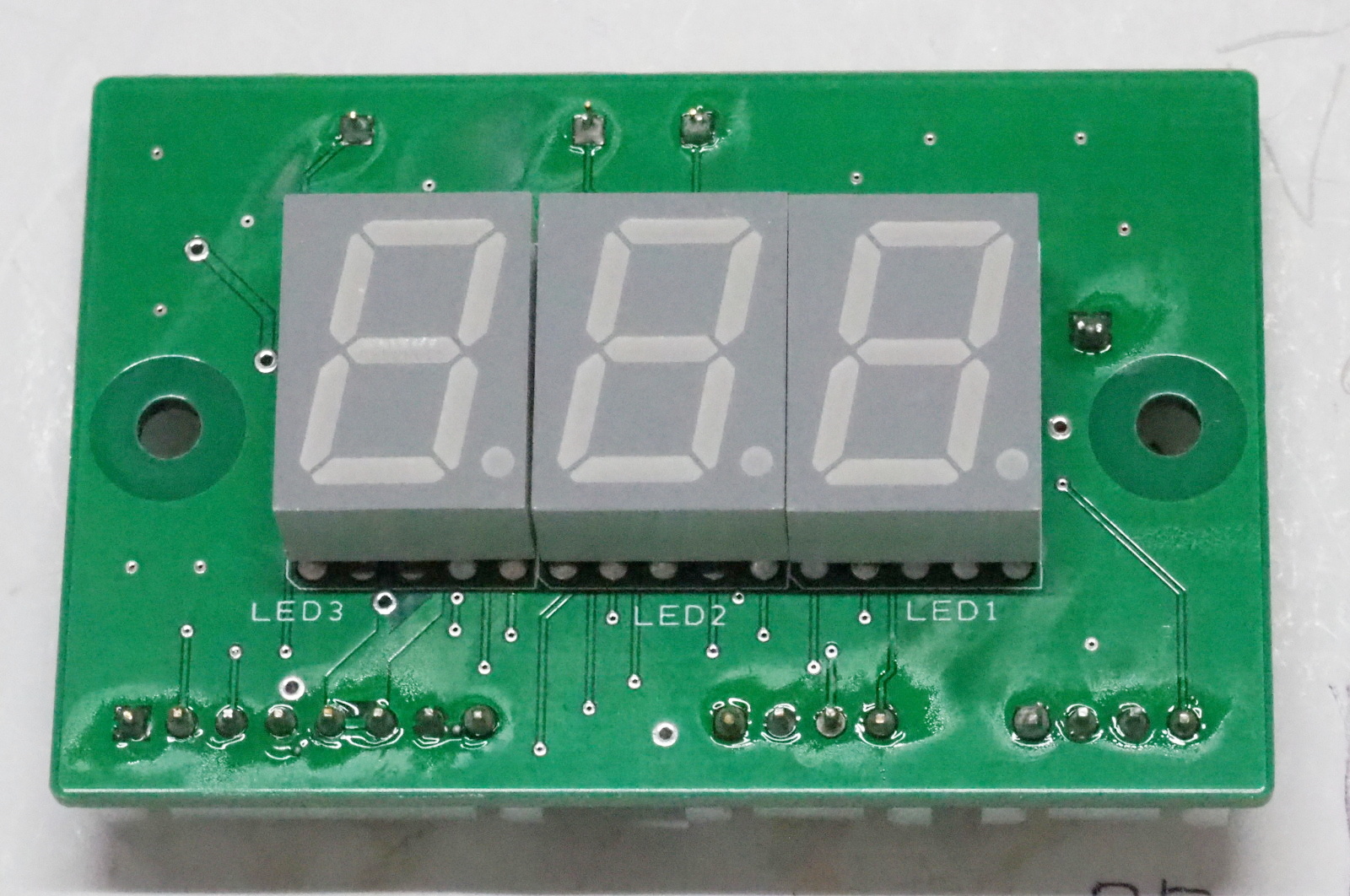
BD1: CC-218 DISP
Display Board that includes three units of 7-segment LEDs (hearafter 7-seg)
and a display controller chip.
<CC-218 DISP specifications: CC-218_DISP_Spec.pdf>
The display controller used is Austria Microsystems (AMS) AS1115. The package type is QSOP-24. It can control up to eight digits of 7-segment displays and read up to 16 switches. Although reading switches may seem simple, it actually requires rather troublesome processing, such as debounce handling. AS1115 performs debounce and notifies MCU via an interrupt when it detects a change in switch state. This eliminates the need for MCU to constantly monitor the switch states.
I had wanted to use orange 7-seg, but chose the ordinary red 7-seg as explained in "Appearance Design". It's Broadcom HDSP-H153.
The block diagram of this board is shown below.
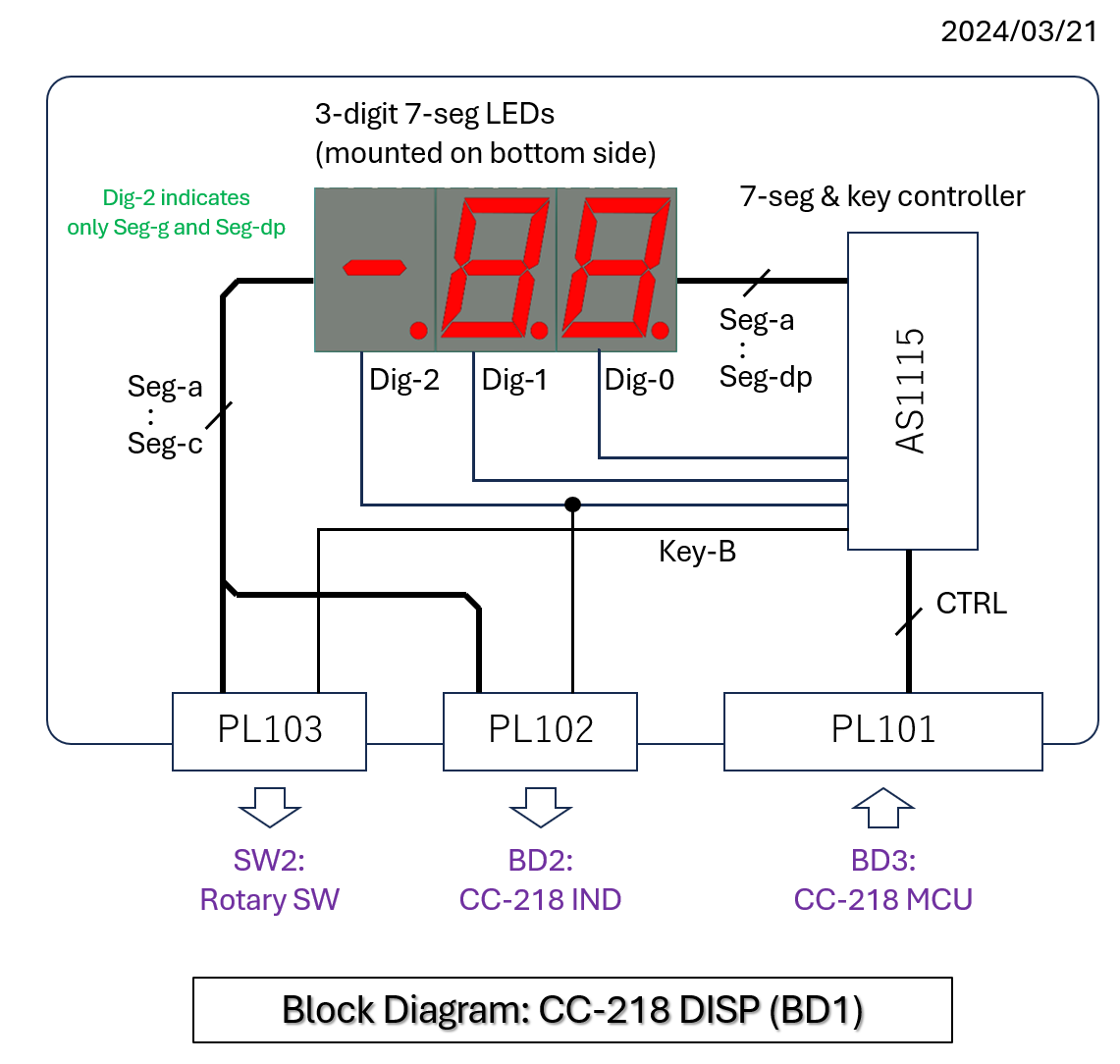
The connector PL101 receives not only control signals but aslo DC power supply from the controller board (CC-218 MCU).
The most significant digit of the numeric display (Dig-2) is used only
to display the minus sign ‘-’ (Seg-g) and the decimal point ‘.’ (Seg-dp).
Seg-a of Dig-2 is used as PHONO Indicator, Seg-b as DAC Indicator, and
Seg-c as AUX Indicator.
The indicators (LED) are mounted on Selector Indicator Board (BD2 CC-218
IND). The signals for the LEDs are output to BD2 via PL102.
The signals for reading the switches are connected to Rotary SW (SW2) via PL103.
The schematic of this board is shown below.
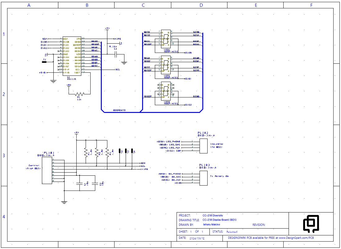
The current-limiting resistor R4 for the LEDs is set to 12 kΩ, resulting in IF (forward current) of 40 mA. Though this may seem like a large current, the LED light needs to pass through the stickers (ST1, ST2), and since the duty cycle is 33%, I concluded that this level of current was necessary.
A rotary SW (Fujisoku SRF113-Z) is used for the selector switch. Since SRF113-Z is a non-shorting type, N-key rollover feature is not required to read the on/off state of the contacts. Therefore, diodes for preventing reverse current are omitted.
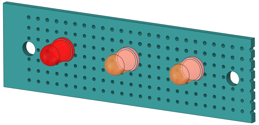
BD2: CC-218 IND
Selector Indicator Board that contains only three LEDs.
BD2 is the only board that uses a universal PCB among the boards in CC-218.
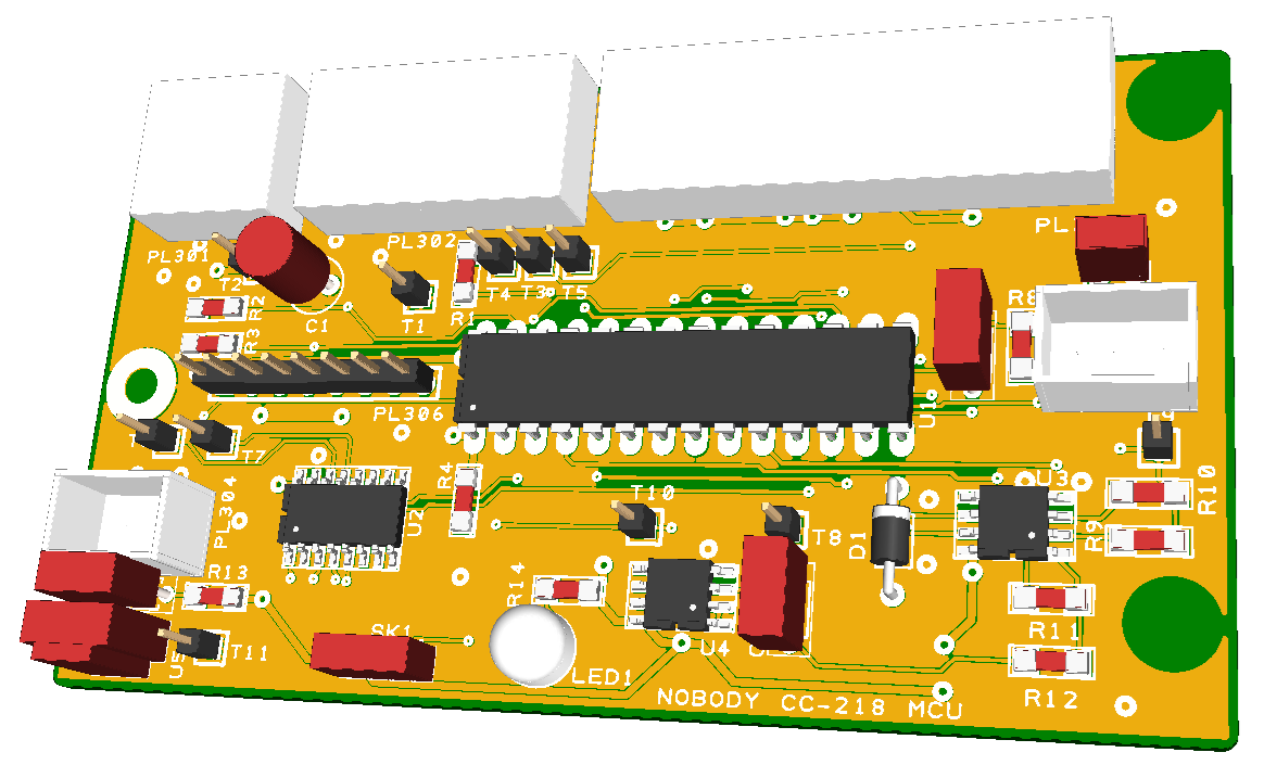
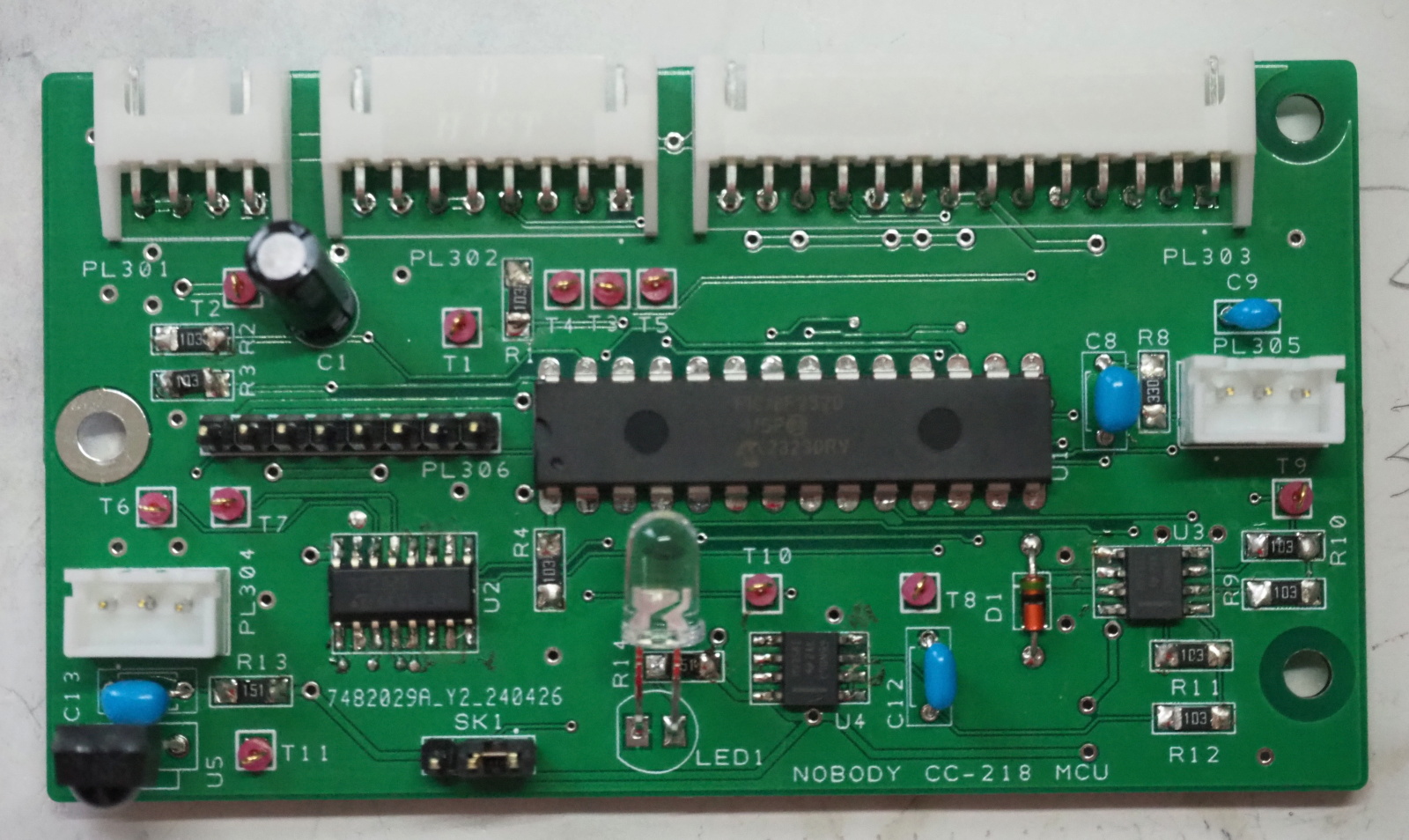
BD3: CC-218 MCU
Controller Board that includes MCU chip, relay drivers, VR interface, and
so on.
<CC-218 MCU Specifications: CC-218_MCU_Spec.pdf>
I selected PIC18F2520 for the MCU chip. The reason of the selection is
mentioned in "Key Parts and Materials".
The package is 28P DIP.
For the relay driver, I chose the GSF2301 P-channel MOSFET from Good-Ark Semiconductor. It has a low on-resistance of 110 mΩ, and a built-in protection diode. So it is easy to use. Another advantage is its low price—just 44 JPY per unit.
A 10 kHz square wave is output to the variome (VR1), generated using MCU’s PWM function. To prolong the contact life of the VR, the output is AC-coupled using a coupling capacitor to remove the DC component. The voltage divided by the VR is then rectified, smoothed, and supplied to the analog input terminal of MCU.
For the infrared receiver (IR receiver), I selected Vishay TSOP34838, but
this turned out not to be the best choice. It’s an older model that is
nearing the end of its production, and I should have opted for the improved
version, TSOP34438, instead. The TSOP34438 is designed to be more resistant
to infrared noise from sources such as inverter-based fluorescent lights.
As of Julyl 2025, it has been in use for about six months, and so far its
operation has been stable. In fact, the air conditioner remote control
used in the same room has far more errors. Since the TSOP34838 and TSOP34438
are pin-compatible, I could still switch them out if necessary, but it
doesn’t seem needed at this point.
At the start of the project, I had very little knowledge of infrared remote
control specifications. , I selected this IR receiver based on the knowledge
I learned from a reference [Ref-42, pp.263~274]. With it, the system can
receive infrared signals from all Japanese-made TV remote controls.
<Reference list>
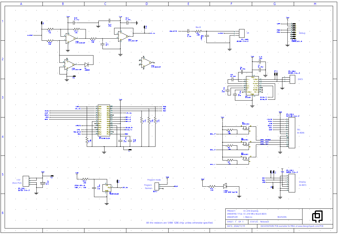
For the rectifier circuit, I chose LMV358IDR, a single-supply, rail-to-rail type op amp. To avoid voltage drop caused by the forward voltage (VF) of the rectifier diode, I contrived this rather complex circuit.
I used a circuit simulator Micro-Cap Ver.12 for debugging this circuit.
<Circuit design document: CC-218_MCU_CircuitDesign.pdf>
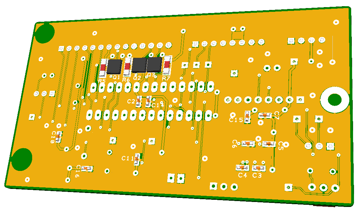
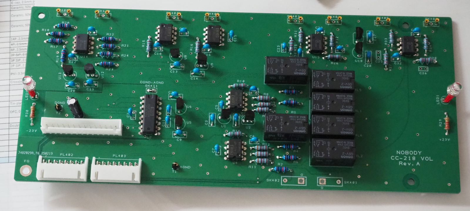
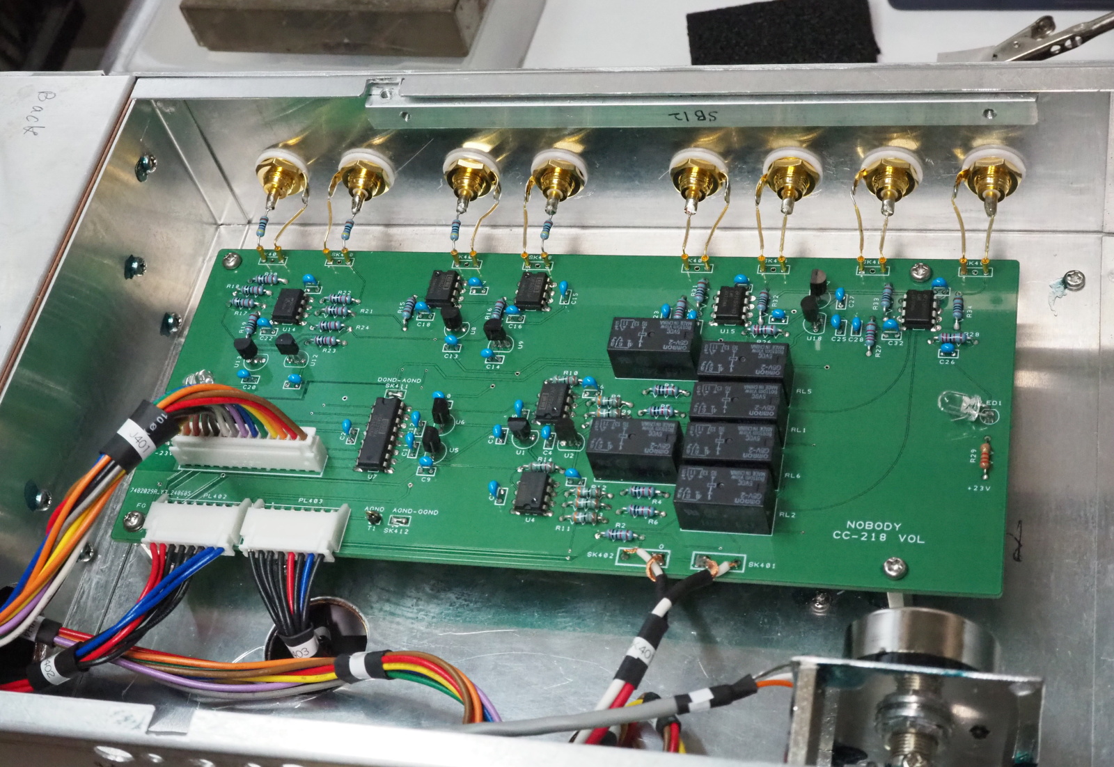
BD4: CC-218 VOL
The selector/volume board that includes the eVolume chip (PGA2310) and
the selector relays.
It's the only board in CC-218 which is composed of both digital and analog
circuits.
<CC-218 VOL Specifications: CC-218_VOL_Spec.pdf>
The selector uses a shunt method, so the audio signal does not pass through
any contacts. Signals from unselected sources are grounded to prevent them
from being output.
I also considered a method using semiconductors as switches (analog switches),
but I couldn’t find a suitable device, so I settled on the shunt method.
In designing this selector circuit, I referred to the book written by Mr.JLH
(John Linsley Hood) (Ref-37, pp.136~137)
<Reference list>
The schematic below is Rev.B (the final revision). Two issues discovered during testing were corrected, resulting in this Rev.B.
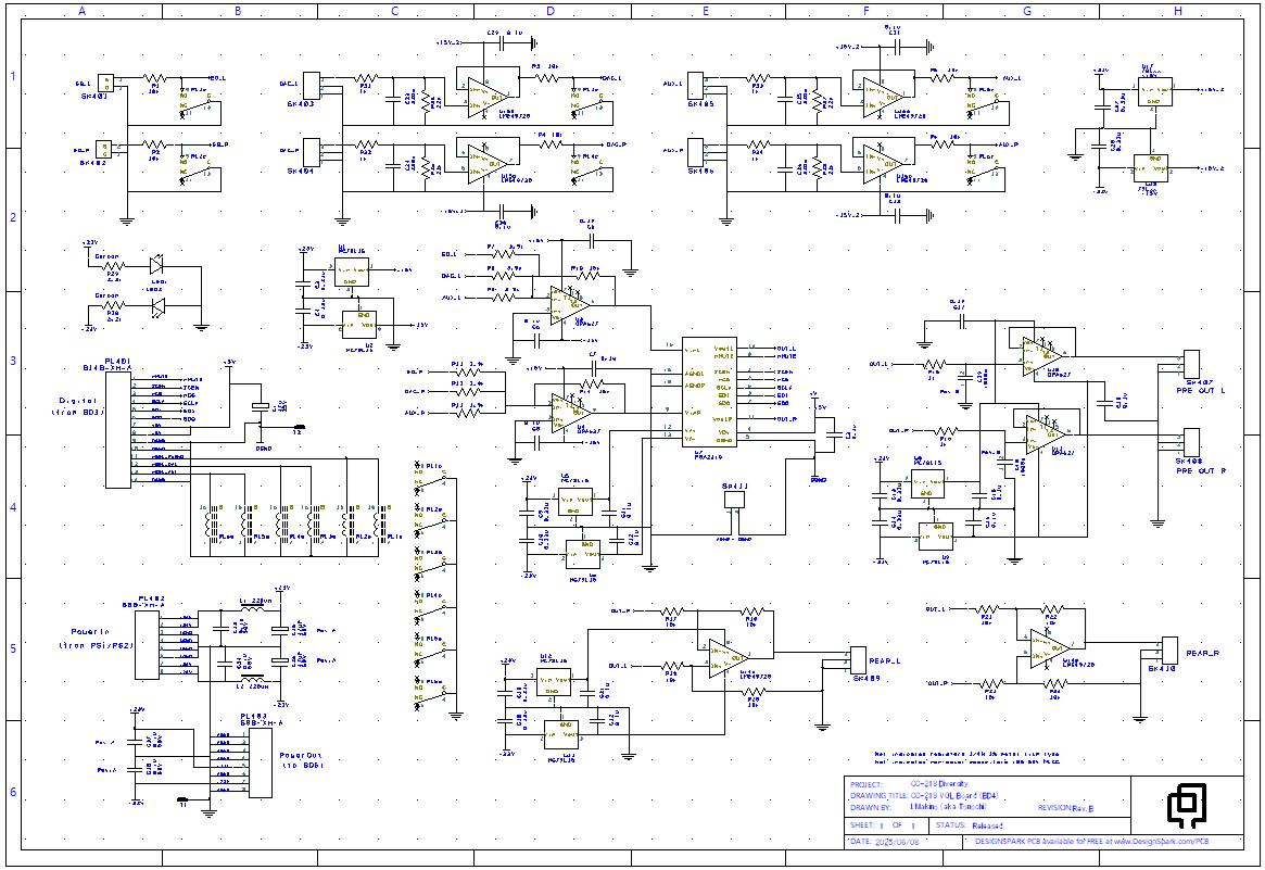
For the selector relay, I chose the Omron G5V-2 mini relay. I also considered using low on-resistance MOSFETs, but relays are easier to use since they are non-polarized, so I went with that option. I am aware of the potential for aging-related degradation. While increased on-resistance could cause slight crosstalk between sources, this only becomes an issue when multiple sources are played simultaneously, which I consider an acceptable shortcoming.
In the previous project (PA-210), I used micro relays, but that was a mistake based on a misunderstanding.
I had simply assumed that relays with smaller form factors were better
suited for switching small signals.
Relay contacts can have a shortened lifespan if the current is too low.
Audio signals generally carry very small currents. For example, applying
1V across a 10kΩ load results in a current of just 0.1 mA, and it's rare
for audio signals to exceed that. Relays used for switching audio signals
must be able to handle low currents.
I considered two candidates: G5V-1 and G5V-2. Both are manufactured by
Omron. G5V-1 is a micro relay, and G5V-2 is a mini relay (with larger form
factor than G5V-1).
The current range for G5V-1 is 1mA ~ 1A, whereas G5V-2 can handle 10µA
~ 2A. As you can see, larger relays tend to support a wider range of current
and are more capable of handling low current. Based on this reasoning,
I chose G5V-2.
According to the datasheet, the contact resistance of G5V-2 is 50mΩ. Based
on that value, the crosstalk between sources calculates to about –94dB.
As the contacts age, this value will worsen. Some amplifier enthusiasts
might find this unsatisfactory, but since I’m not one of them, I have no
intention of chasing excessive performance—I’m satisfied with this.
<Circuit design document: CC-218_VOL_CircuitDesign.pdf>
The revisions are summarized below. For details, please refer to “Measurements and Improvements.”
Rev.A: A noise filter was added to the DC power line, which I had forgotten
in the original design. The GND wiring was changed from bus-bar to ground
plane.
Rev. B: An LPF (low-pass filter) was added to the output buffer. Since this change
does not require any modification to the PCB, the PCB (PCB4) remains as
Rev.A.
U7(PGA2310):P7(SDO) is connected to PL401:P6, but this is a mistake due to a misunderstanding. SDO (Serial Data Output) pin is meant to be connected to the SDI (Serial Data Input) of another PGA2310 when using multiple PGA2310s. Connecting it to MCU is no use, so MCU (to be more precise, firmware of MCU) simply ignores this signal.
BD5: CC-218 EQ
Phono equalizer board designed specifically for MC-type cartridges.
It combines an ultra-low-noise op amp, LT1115, with passive filters. The
gain is set slightly higher than the industry standard, at 66dB (@1kHz).
<CC-218 EQ Specifications: CC-218_EQ_Spec.pdf>
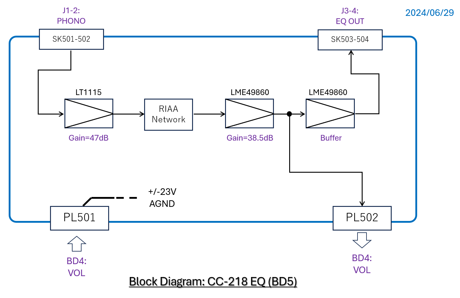
This circuit is not my original design; it is based on an application example featured in the LT1115 datasheet. The only difference is that the gain of the second stage has been increased by 10dB. While the application example naturally uses only LT op amps, I used TI's LME49860 for all stages except the first.
The output is not only sent to BD4 (CC-218 VOL), but also routed to the RCA jacks (EQ OUT (J3, J4)) on Back Panel via the buffer (voltage follower). So, CC-218 can be used as a standalone phono equalizer, too.
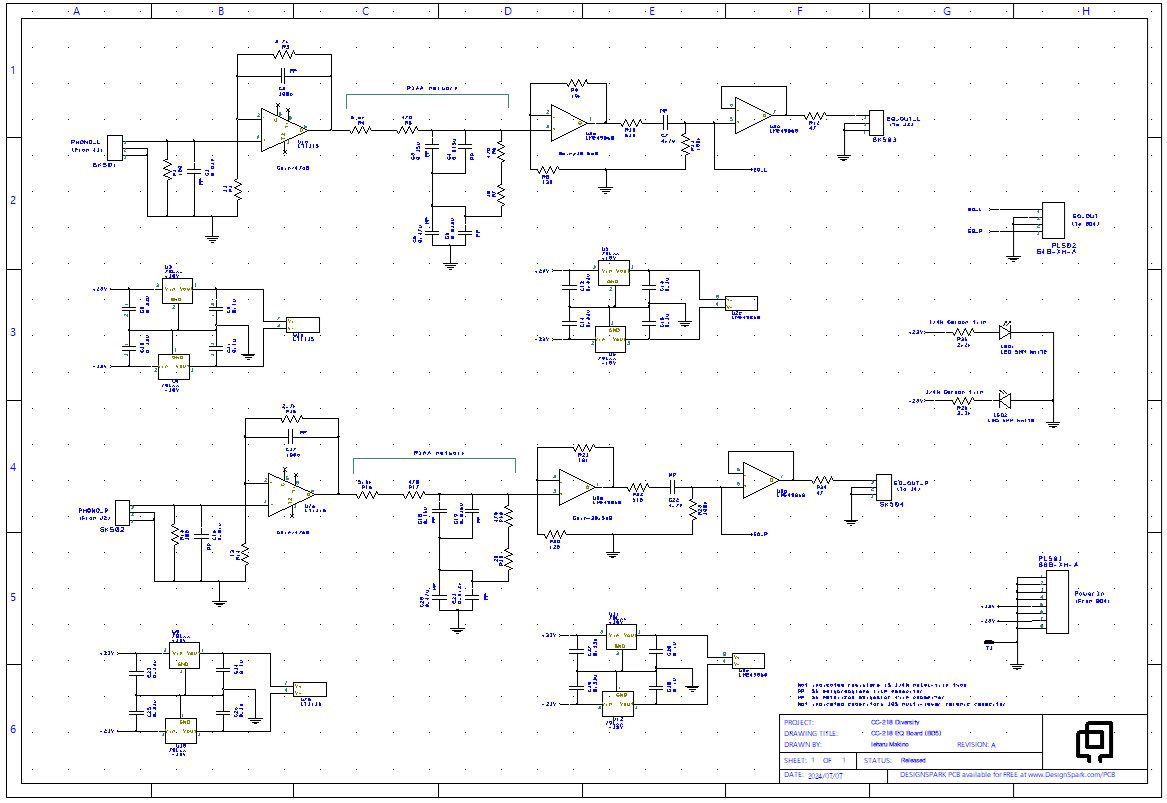
The resistors used in the RIAA network have a tolerance of 1%, and the
capacitors have a tolerance of 5%. Since the resistor and capacitor values
are selected from the E24 and E12 series, respectively, they deviate from
the calculated ideal values. To get as close as possible to the calculated
values, two resistors were connected in series and two capacitors in parallel.
Even so, there were still slight discrepancies, so I verified the characteristics
through simulation.
In the simulation result shown below, the input signal has RIAA-compliant
pre-emphasis applied. If the output appears flat, it indicates that the
characteristics are correct.
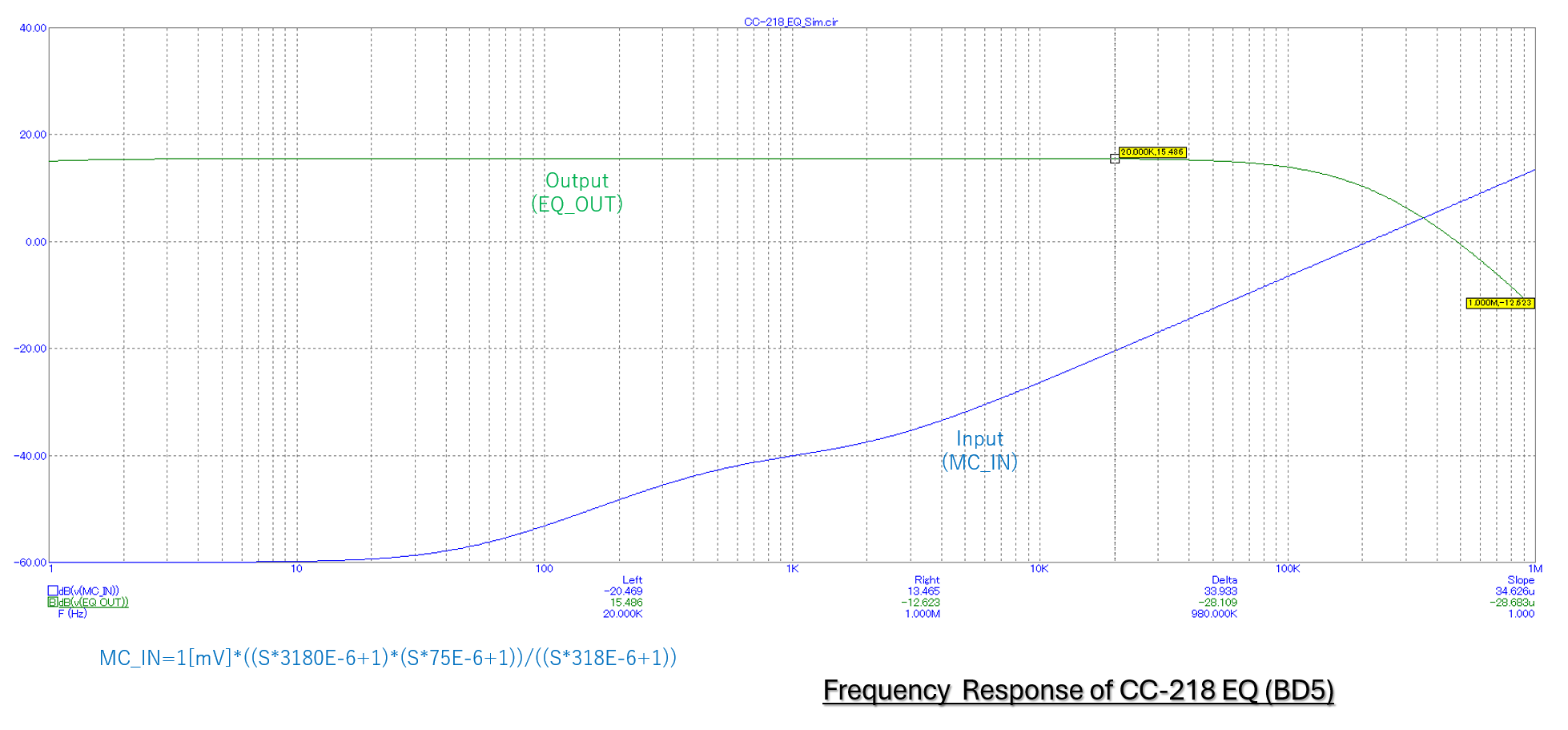
The RIAA deviation came out to be –0.045dB to +0.023 dB (20Hz ~ 20kHz), which is an excellent result.
For the op amps, I selected audio-grade components, but for the passive
components, I also used non-audio-grade parts.
The resistors are basically audio-grade metal film resistors (REY series)
by Takman. However, since this series has been discontinued, some resistance
values were difficult to obtain. As substitutes, I used KOA’s general-purpose
metal film resistors (MF1/4C). There’s not much difference in specifications
between the two, but Takman uses OFC leads.
For the capacitors used in the RIAA network, I selected polypropylene capacitors
(UPZ series) from Nichicon. However, for larger capacitance values (0.47 µF
and 4.7 µF), I used metallized polyester capacitors (ECQE series) by Panasonic.
There’s no particular reason for this choice—it simply met the requirements
of being a film capacitor with 5% tolerance, rated at 50V or more, and
readily available at the time.
Using Vishay’s audio-grade resistors or WIMA’s audio-grade capacitors might have appealed more to audio enthusiasts, but lately, I’ve stopped being particular about using audio-specific components.
Rev.A:
Although the ECQE capacitors with a 100 V rating would have been sufficient,
they seemed to take quite a while to source, so I opted for the 250 V version
instead. However, their physical size is considerably larger, making it
difficult to mount them on the already-ordered PCB (PCB5). As a result,
I modified the PCB to accommodate the 250 V parts. It may sound odd to
say that modifying the PCB is easier than changing the capacitors, but
that’s honestly how it felt. The PCB cost about 3,200 JPY including shipping,
which isn’t much different from buying 10 audio-grade capacitors. Even
from an economic standpoint, I didn’t feel burdened by the revision.
<Circuit design document: CC-218_EQ_CircuitDesign.pdf>
PCB Design
PCB1: CC-218 DISP
I assumed it would be easy to design the PCB, since it’s a simple board
with just one IC, three 7-seg LEDs, and three connectors—but that was a
big mistake. It ended up taking five whole months. Even though it was my
first time designing a PCB, I never expected it to be this much trouble.
The AS1115 in a QSOP-24 package has a pin pitch of only 0.4mm, and with
such dense traces around it, it’s difficult not only to add through-holes
but even to place vias. In addition to that, most of the space on the bottom
side was taken up by the 7-seg LEDs, making it hard to place decoupling
capacitors near the AS1115.
At first, I planned to use the auto-routing function of the CAD software
(DesignSpark PCB), and if there were any nets that didn’t get connected,
I would manually route just those remaining nets myself. However, this
approach didn’t work.
In reality, there were nets that the auto-router couldn’t connect. And
if even a computer couldn’t figure it out, there was no way I could. Trying
to route a single trace meant I had to move another one, which then required
moving yet another trace to make space—and in the end, I had to start over
from scratch.
In the end, I couldn’t fit all the traces no matter what I did, so I ended up changing the board dimensions. I extended the height by 8 mm.
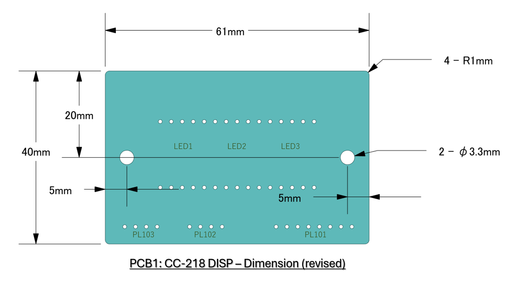 |
| The height has been changed from 32mm to 40mm |
To place the decoupling capacitor for the power rail near the AS1115, I used a little trick: I mounted the capacitor so that it straddles over the top of the AS1115.
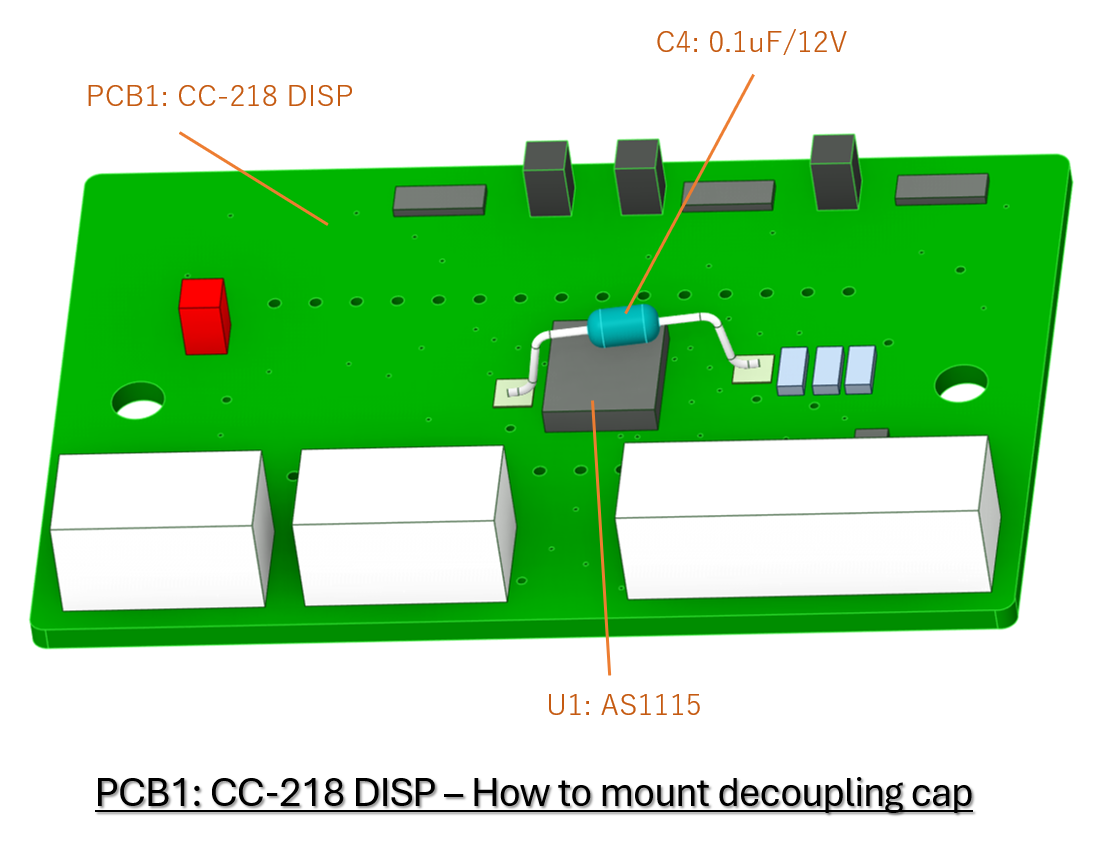 |
| Mount the capacitor (C4) so that it straddles over AS1115. Place pads of +5V and GND near AS1115. The cap is soldered to the pads. |
For further details of designing this PCB, see the document below:
<PCB design document: CC-218_DISP_PCB.pdf>
The images below are renderings of the completed board generated by the PCB CAD software.
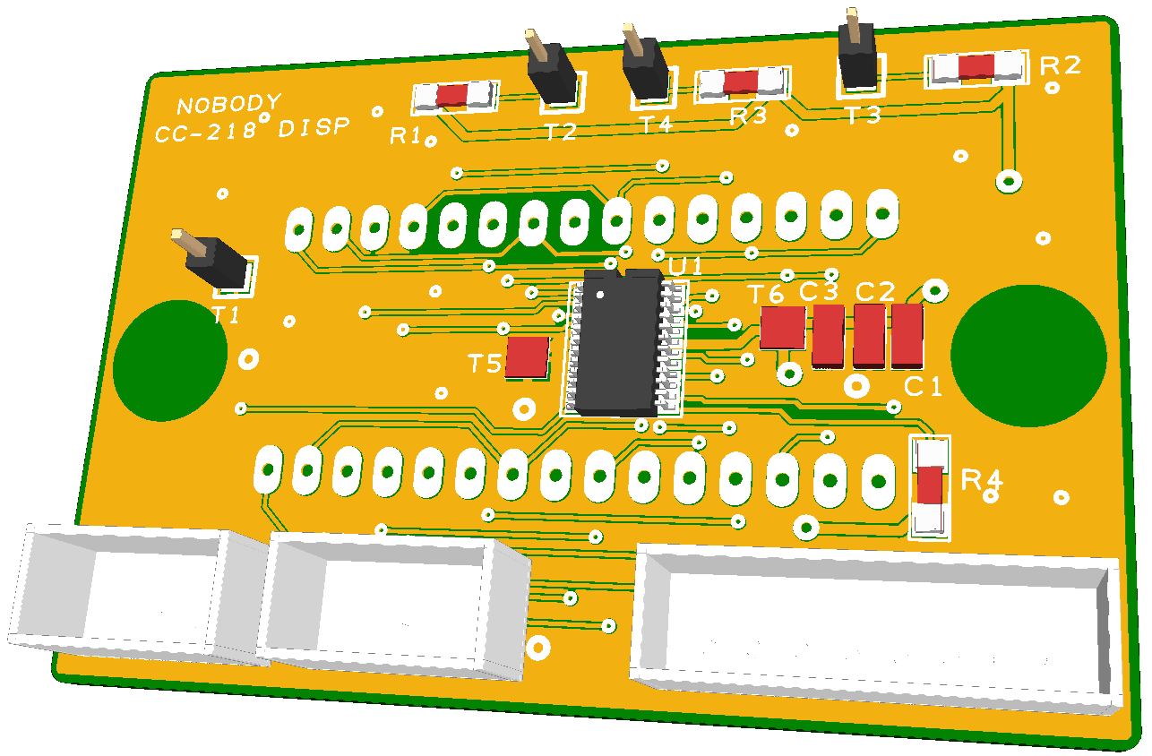 |
 |
| Rendering created by PCB CAD - CC-218 DISP (top) | Rendering created by PCB CAD - CC-218 DISP (bottom) |
PCB3: CC-218 MCU
Compared to PCB1, this board has many more components, yet its area is
only slightly larger. So, I expected it to be even more challenging than
PCB1, but surprisingly, the design progressed smoothly. I completed the
design in about five weeks. I was becoming more proficient in PCB design.
<PCB design document: CC-218_MCU_PCB.pdf>
 |
 |
| Rendering created by PCB CAD - CC-218 MCU (top) | Rendering created by PCB CAD - CC-218 MCU (bottom) |
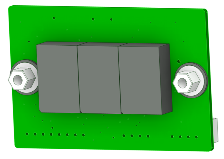
PCB4: CC-218 VOL
This is my first time designing a PCB that includes analog circuits. I considered changing the design rules, but in the end, decided to keep most of them unchanged. The main modification was making the trace widths for analog signals and analog ground (AGND) wider than those for digital circuits. Specifically, the analog signal traces are 0.2mm wide (compared to 0.152mm for digital signals), and the AGND is 1.8mm wide (compared to 0.5mm or 1.2mm for DGND).
I carefully designed the routing of AGND, but the 1.8mm trace width doesn’t provide sufficiently low impedance. Therefore, I decided to reinforce it with 1mm tin-plated copper wires.
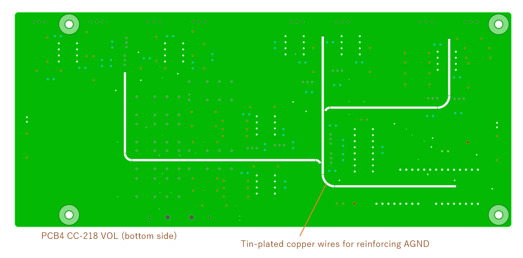 |
| AGND is placed on the bottom side, with portions of the solder mask removed
along its track. The tin-plated wire is soldered onto the exposed areas
of the track. This design was rejected later! |
A guard ring should be placed around the input pins of op amps. To implement this, I used the available space on the top layer as guard ground (GGND) plane, which prevents crosstalks between signals. GGND is connected to AGND at a single point.
I decided not to employ this AGND and GGND design when revising this PCB to Rev.A. Although the purpose of Rev.A was not related to AGND, I deleted GGND plane, and poured copper in the availabe spaces on both sides and designated them as AGND planes, because using AGND planes on BD5 (Phono EQ board) had yielded good results.
Rev.A
A noise filter was added to the ±24V DC power rails. All the components
of the filter are SMDs (surface-mount device) and are mounted on the bottom
side near connectors PL402 and PL403.
AGND tracks were also changed to the AGND planes.
<PCB design document: CC-218_VOL_PCB.pdf>
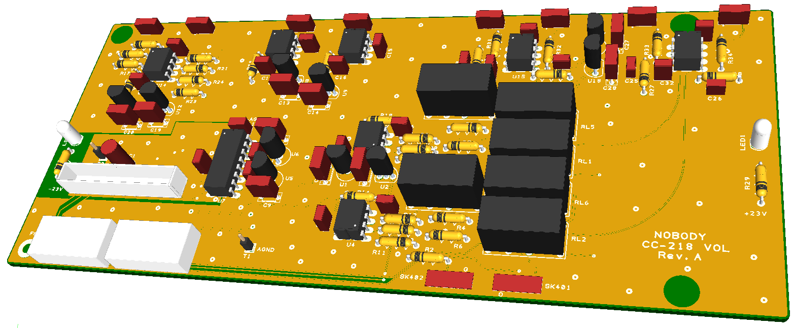 |
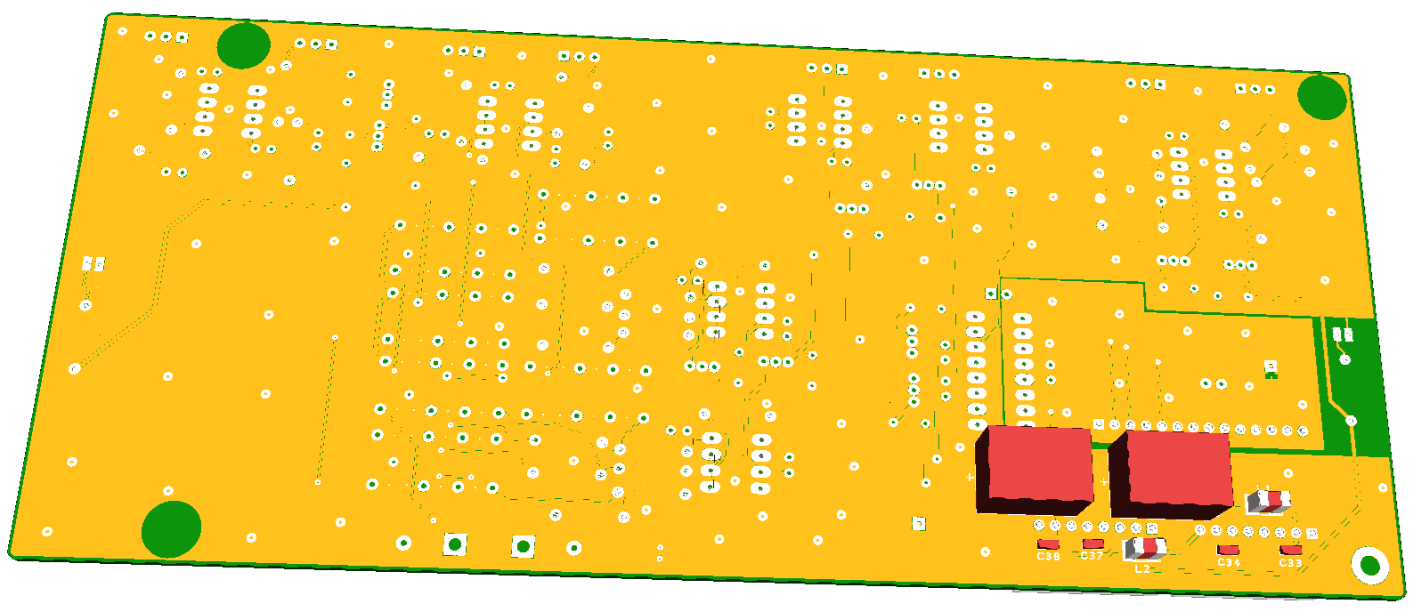 |
| Rendering created by PCB CAD - CC-218 VOL (top) | Rendering created by PCB CAD - CC-218 VOL (bottom) |
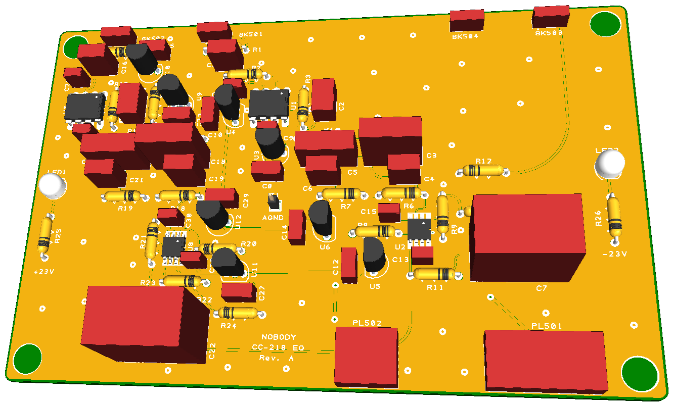
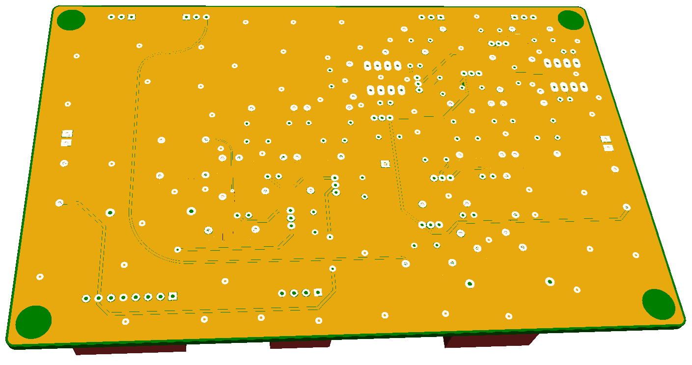
PCB5: CC-218 EQ
Since this is a high-sensitivity amplifier with an input sensitivity of
0.3mV, even the best circuit design will result in a bad sound quality
with noise and distortion if the PCB design is poor. I felt quite a bit
of pressure during the PCB design process. What I struggled with most was
the GND routing. At one point, I even considered switching to a poured
GND plane. In an amplifier that handles extremely small signals, even a
1 μV fluctuation in GND potential can cause audible noise. An ultra-low-noise
amplifier needs GND that is as stable and immovable as the Earth itself.
However, one thing kept nagging at me—a lesson I learned from senior engineers
long ago: Never use GND plane in low-frequency amplifier circuits. The
reasons include: (1) Currents from multiple amplification stages can overlap
within the GND plane. (2) Stray currents can flow through GND. (3) Eddy
currents can develop within GND plane. (4) Increased stray capacitance
between the signal and GND tracks can cause phase shifts and attenuation
at high frequencies.
The issue in point (1) is that the impedance within the GND plane becomes a common impedance, leading to crosstalk between circuits. However, the impedance of the GND plane is sufficiently low, and the level of crosstalk can be considered completely negligible. Points (2) and (3) are thought to potentially cause signal waveform distortion, but it’s unlikely that distortion of any significant magnitude would actually occur. Point (4) can be completely dismissed. If stray capacitance were to cause phase shifts within the audible frequency range, then GND planes could not be used in digital boards. In reality, however, GND planes are a standard technique used in nearly all digital PCBs. That said, if the output impedance of an amplification stage is high, the effects of stray capacitance might become noticeable.
<PCB design document: CC-218_EQ_PCB.pdf>
 |
 |
| Rendering created by PCB CAD - CC-218 EQ (top) | Rendering created by PCB CAD - CC-218 EQ (bottom) |
BOMs and Assembly Manuals
BOM (Total)
<BOM: CC-218_BOM.pdf>
BOMs of the boards
<BOM of Display Board: CC-218_DISP_BOM.pdf>
<BOM of Indicator Board: CC-218_IND_BOM.pdf>
<BOM of Controller Board: CC-218_MCU_BOM.pdf>
<BOM of Volume Board: CC-218_VOL_BOM.pdf>
<BOM of Phono EQ: CC-218_EQ_BOM.pdf>
Assembly manual (Total)
<Assy manual: CC-218_Assy.pdf>
Assembly manuals for the boards
<Assy manual for Display Board: CC-218_DISP_Assy.pdf>
<Assy manual for Indicator Board: CC-218_IND_Assy.pdf>
<Assy manual for Controller Board: CC-218_MCU_Assy.pdf>
<Assy manual for Volume Board: CC-218_VOL_Assy.pdf>
<Assy manual for PhonoEQ Board: CC-218_EQ_Assy.pdf>
 |
 |
| Rendering of Display Module |
Rendering of Indicator Module |
 |
 |
| Rendering of VR Module | Rendering of Rotary SW Module |
Firmware Design
This firmware (F/W) is named 'CC-218 FW'.
Development environment and programming language
I use IDE (Integrated Develop Environment),which is the free software offerred by Microchip.
Development environment: MPLAB X IDE v6.20
Compiler:XC8 v2.50 (language C)
Debugger/programmer:MPLAB PICkit 5 (ICD: In-Circuit Debugger/programmer)
I write the entire source code in C. To avoid the need for using assembly language, XC8 provides directives (such as #pragma config) and macros (such as CLRWDT()) for handling operations that cannot be written in standard C.
I purchased the PICkit 5 from Digi-Key for 16,378 JPY. It was cheaper than
buying it from the Microchip Store.
The in-circuit method refers to running the firmware using the MCU chip
on the target system. For this, the firmware needs to be built specifically
for debugging. When built as a debug version, the firmware has debug-related
code linked in, which slightly increases memory usage and may slow down
execution speed.
Using an ICE (In-Circuit Emulator) allows real-time execution without modifying
the firmware, but it's quite expensive (around 200,000 JPY ?).
Note that the term “programmer” here does not refer to a person who writes
code, but rather to a device that writes programs or data into the flash
memory of a microcontroller chip.
As will be explained in the section on “Debugging Method,” in-circuit debuggers are only suitable for very simple firmware that
doesn’t use interrupts. The main purpose of the PICkit 5 is programming
rather than debugging.
Basic structure
Generally, firmware for an amplifier is relatively simple and does not
require high real-time performance, so I adopted a simple structure without
using an RTOS (Real-Time Operating System). This is what’s called a stand-alone
approach.
Unlike regular software, firmware does not terminate. It continues running
as long as the target system is powered on. As shown in the left part of
the flowchart below, after completing initialization, it enters the infinite
loop. Within this loop, each task is executed.
Formally, this program structure is single-task, but with a bit of ingenuity,
it can behave like a multitasking system.
Each task has to be designed so that it does not wait for events. Events
refer to things like changes in input port states or interrupt requests
from peripherals. If a task waits for an event within itself, it ends up
occupying the CPU for too long, which delays the execution of other tasks.
Before executing each task, the program checks whether the conditions for
running that task are met. If not, it moves on to the next task. As long
as one iteration of the infinite loop completes in at most a few tens of
milliseconds, the system can appear to operate like a multitasking one.
This approach is sometimes referred to as “pseudo-multitasking.”
Tasks
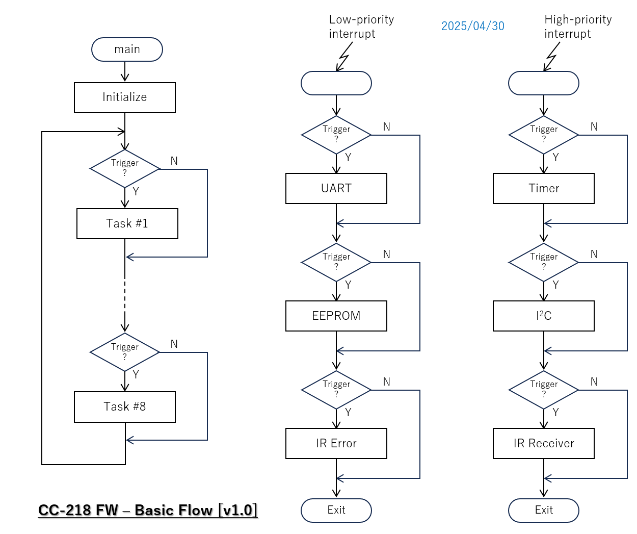
CC-218 FW includes eight tasks.
| Task # | Task name | Trigger | Action |
|---|---|---|---|
| 1 | Execute Console Command | Receive command from Console | Analyze and execute command |
| 2 | Execute Remote Command | Receive command from Remote | Analyze and execute command |
| 3 | Execute Test Program | When F/W is in Diag Mode (*1) | Execute test program (*2) Exit Diag Mode if test is over |
| 4 | Execute Test Program at Tick | Diag Tick (*3) is generated in Diag Mode | Execute test program Exit Diag Mode if test is over |
| 5 | Gain Control | Main Tick (*4) is generated after VR1 (*5) is operated |
Calculate target gain from the angle of VR1 Set the target gain to eVolume chip Display the gain |
| 6 | Selector Control | Main Tick is generated after SW2 (*6) is operated | Read SW2 and recognize which source to be selected Drive Selector Relays Indicate the selected source |
| 7 | Muting | Main Tick is generated during Muting Mode | Decrease or increase the gain Display the gain |
| 8 | Display Timeout | 3 seconds elapsed since the last change of Display | Turn off Display in certain Display Modes |
*1: Diagnostics Mode is one of four modes (the others are Stand-alone Mode,
Master Mode and Balance Adjust Mode) of CC-218 FW, where test programs
are executed. The only way to enter Diagnostics Mode is receiving test
program commands from Console.
*2: Test programs are used to check hardware and/or firmware. Only some Console
commands invoke them. The test programs are, so to speak, "easter
egg" (hidden feature).
*3: Diag Tick is a timing signal for the test programs. It is generated at
1sec intervals.
*4: Main Tick is a timing signal for the main routine (main()). It is generated
at 0.1sec intervals.
*5: VR1 is the variable resistor rotated by Volume Knob.
*6: SW2 is the rotary switch rotated by Selector Knob.
Interrupts
When a response must be made in a very short time after an event occurs,
interrupts are used.
PIC18F2520 has two levels of interrupt priority. High-priority interrupts
are used for processing that requires more urgency, while other events
are handled by low-priority interrupts.
Note that PIC18F2520 does not support NMI (non-maskable interrupt).
Low-priority interrupts
| ISR (*1) | Source | Event | Action |
|---|---|---|---|
| UART(*2) Transmit |
UART (EUSART(*3)) |
Tx Register is empty (Transmit is ready) | Transfer one byte of data from FIFO(*4) to Tx Register, if FIFO is not empty |
| UART Receive |
UART (EUSART) |
Rx Register is full (Receive is ready) | Transfer one byte of data from Rx Register to FIFO |
| EEPROM(*5) | EEPROM | Write is done | Check if error occurred or not |
| IR Error | Timer1 (*6) | Overflow of Timer1, which means disruption of IR signal | Reset the state machine (*7) of IR Remote Driver (*8) |
*1: Interrupt Service Routine
*2: Universal Asynchronous Receiver/Transmitter -- Peripheral device that
executes asynchronous serial communication (a part of EUSART)
*3: Enhanced Universal Synchronous/Asynchronous Receiver/Transmitter -- Peripheral
device that executes serial communication (built-in device of MCU chip)
*4: First-In First-Out buffer -- Data buffer memory in UART Driver
*5: Electronically Erasable and Programmable Read-Only Memory (nonvolatile
memory, built-in device of MCU chip)
*6: Timer/counter (built-in device of MCU chip)
*7: State machine -- Explain later
*8: Device driver that processes signals received from IR remote
High-priority interrupts
| ISR | Source | Event | Action |
|---|---|---|---|
| Timer | Timer0 (*1) | Overflow of Timer0 (at 1msec intervals) | Count down Soft Timer (*2) by 1 |
| I2C | MSSP (*3) | End of transmit/receive | Trigger the state machine (*4) of I2C Driver |
| IR Receiver | PORTB (*5) | Transition of the output of IR Receiver (nIR_IN) | Trigger the state machine of IR Remote Driver |
*1: Timer/counter (built-in device of MCU chip)
*2: Count-down timer in F/W decreased by F/W
*3: Master Synchronous Serial Port -- Built-in serial port of MCU chip. Unlike
EUSART, which commnucates with an external system such as PC, MSSP communicates
with internal devices. It supports SPI mode and I2C mode. The latter is
selected in CC-218 FW.
*4: State machine -- Explain later
*5: I/O port of MCU chip. PORTB receives the signal nIR_IN from IR Receiver
Modules
Now we have definitions of the tasks and ISRs.
It is difficult to include all these tasks and ISRs in a single source
file. So, I divided F/W into modules as shown in the table below.
The expression [vn.nn] indicates the final version numbers of each module.
| Module | Source file | Header file | Description |
|---|---|---|---|
| MAIN | main.c | main.h | The main module including main() |
| INIT | init.c [v0.50] | init.h [v0.52] | Initialize system |
| DIAG | diag.c [v0.31] | diag.h [v0.30] | Self-check programs |
| CNSL | cnsl.c [v0.12] | cnsl.h [v0.11] | Console service routines (UART Driver) |
| INTR | intr.c [v0.05] | --- | Interrupt service routines including I2C Driver |
| DISP | disp.c [v0.23] | disp.h [v0.23] | Display Driver |
| VOLM | volm.c [v0.30] | volm.h [v0.30] | Read VR1, calculate gain data and display the gain |
| REMT | remt.c [v0.10] | remt.h [v0.10] | IR Remote Driver |
State machines
Since firmware is based on event-driven programming, the execution order—aside
from the overall flow—cannot be represented using a flowchart. Instead,
it is helpful to define state machines and use state transition diagrams
to describe the behavior.
CC-218 FW uses three state machines. Only the state transition diagrams
are shown here; for details, please refer to the design documentation.
<F/W design document: CC-218_FW_Design.pdf>
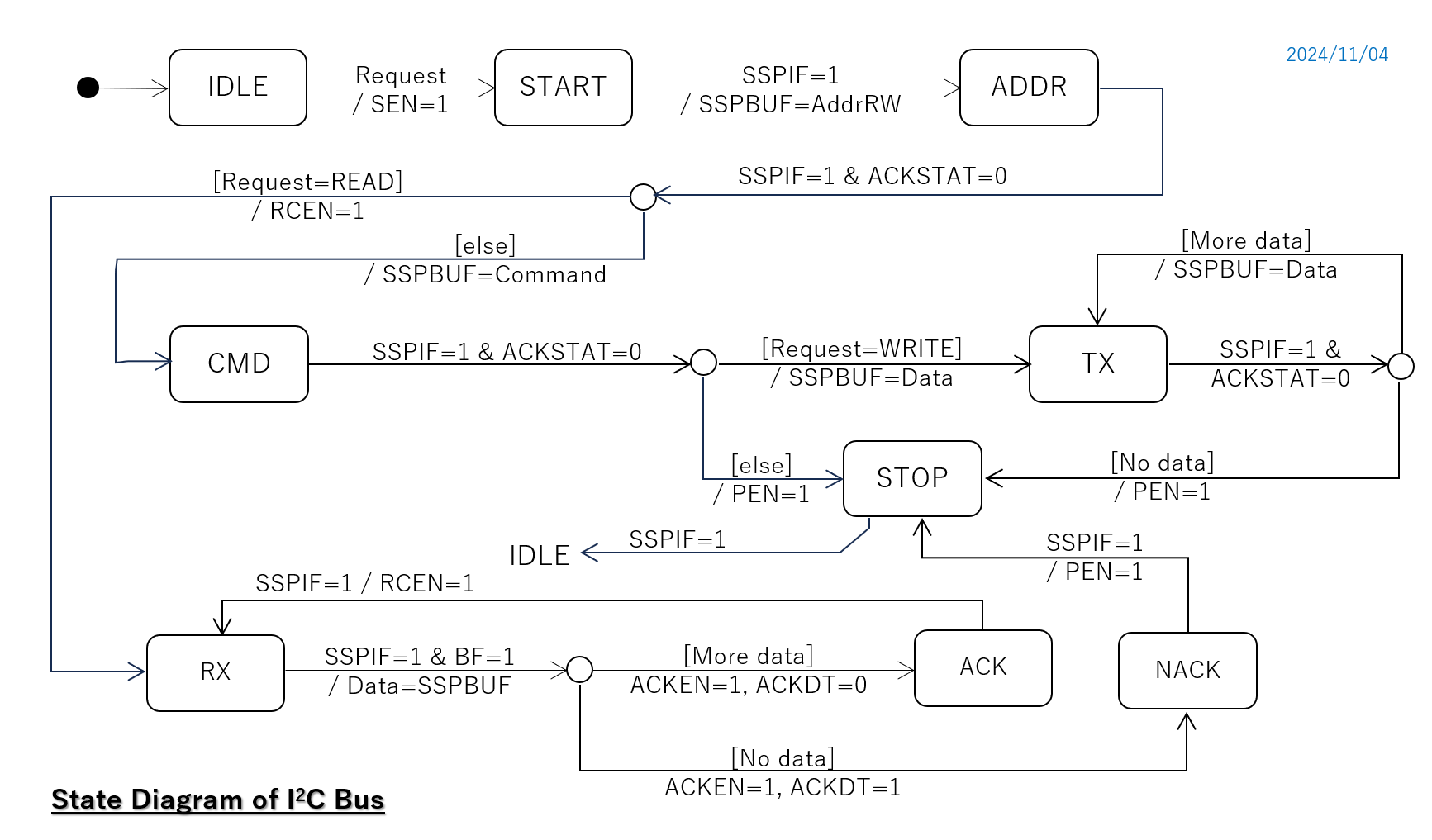 |
| State transition diagram -- I2C Driver |
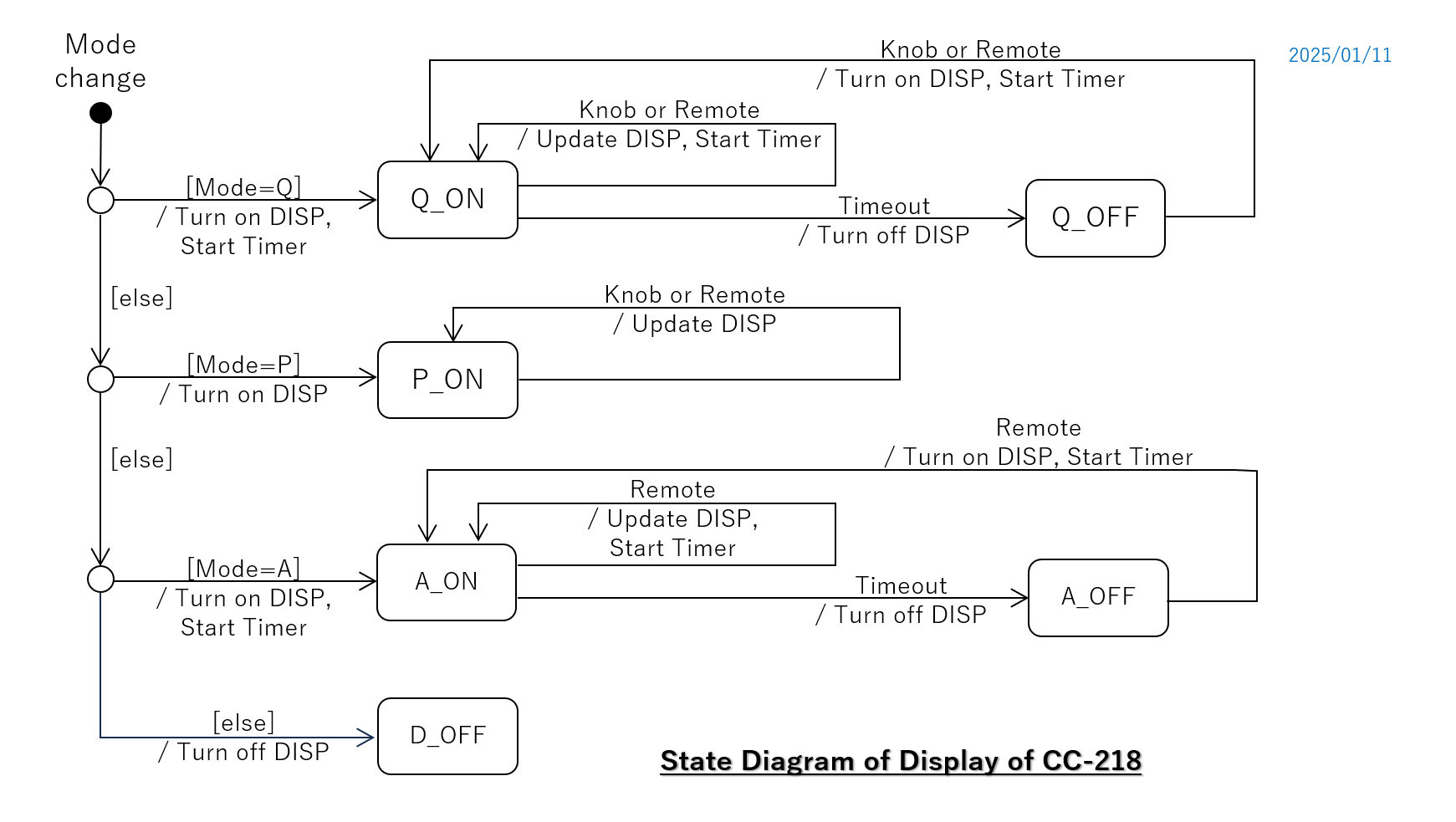 |
| State transition diagram -- Display Driver |
 |
| State transition diagram -- IR Remote Driver |
Design procedure
Firmware tends to be more complex in terms of function and structure than
hardware, so using a design-then-implement approach can lead to confusion.
This is especially true for a project like the CC-218, where both the hardware
and firmware are newly developed—it's hard to know where bugs might be
hiding. Therefore, it's best to follow a step-by-step approach, where design,
implementation, and debugging are carried out in parallel.
First, design and implement firmware with only the minimum required functionality.
Then write it to the target chip, run it, and debug. Once that works, add
one more function to the firmware and debug again in the same way. Repeat
this process until the firmware is complete.
Each step is assigned its own version number.
| Version | Feature | Purpose |
|---|---|---|
| v0.0 | Make the LED connected to PORTC of MCU chip blink with a 2sec cycle | Confirm basic operations of IDE, PICKit (ICD) and MCU chip |
| v0.1 | Connect MCU to Console (Tera Term) by using newly added UART Driver (CNSL Module) | Display the internal status and events of MCU on Console screen |
| v0.2 | Display numeric characters on Display by using the display controller (AS1115)
and newly added I2C Driver (DISP Module) Self-check programs (DIAG Module) added |
Confirm operations of Display and Indicator (BD1 and BD2, respectively) |
| v0.3 | Display the gain data calculated from readings of VR1 on Console screen.
Newly added VR Driver (VOLM Module) is used to read the voltage of VR1. VR Driver uses PWM (*1) and ADC (*2) Display the gain values on Display (BD1) |
Confrim accuracy and linearity of the reading of VR1 Check the gain data to be set to PGA2310 (*3) Check the relation between the gain data and actual gain |
| v0.4 | Send gain data to PGA2310 Drive Selector Relays according to state of SW2 |
CC-218 works as preamp |
| v0.5 | Console Commands are implemented Setting data are saved in EEPROM |
CC-218 can be controlled by Console Settings, such as brightness of Display, can be changed by Console Commands Self-test programs can be invoked by Console Commands |
| v0.6 | IR Remote Driver (REMT Module) is added | CC-218 can be controlled by Remote Commands |
| v0.7 | DVCS Master Mode is implemented | Send commands to DVCS slave device(s) when CC-218 is in Master Mode |
| v1.0 | Final version WDT(*4) enabled |
CC-218 perfectly meets the specifications |
*1: One of the features of CCP Module (built-in peripheral of MCU chip) --
used to generate square wave of 10kHz, 50% duty
*2: 12-bit A/D converter (built-in peripheral of MCU chip)
*3: Electronic volume chip
*4: Watch Dog Timer -- used to reset CPU when it runs away
For further details of the design procedure, refer to the following document.
<F/W design document: CC-218_FW_Design.pdf>
 | |
| Ver.0.00 MCU chip works for the first time |
Ver.0.11 Console (Tera Term 5) connected to CC-218 |
 | |
| Ver.0.21 Display Controller (AS1115) starts working |
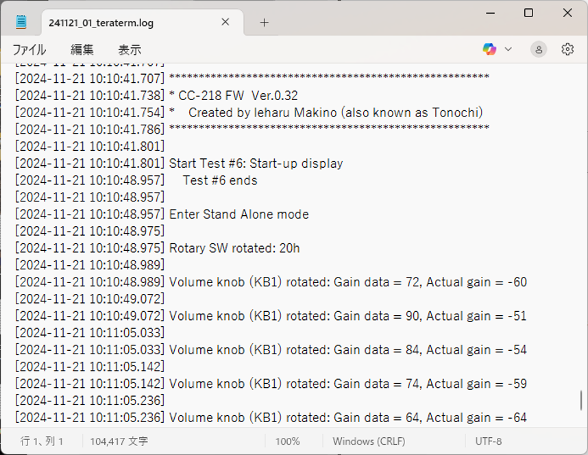
Ver.0.32 Calculating the gain and gain data according to rotation of VOL Knob (Tera Term log) |
 |
|
| Ver.0.50 Now CC-218 works as preamp |
Ver.0.60 IR Remote works |
Debugging method
I believe that the methods for debugging firmware are generally not covered
in programming textbooks. Unlike software debugging—where you use a debugger,
set breakpoints, step through the code, or display variable values—such
methods do not work in embedded systems, which are event-driven and require
real-time responsiveness.
Although I don’t intend to give overly general explanations on this website,
I think firmware design and debugging are largely unfamiliar to audiophiles,
so I’ll offer a brief explanation.
An effective method for debugging firmware is to connect a console to the
target system (CC-218) and display events and status information on the
console screen. What I refer to as "console" is a terminal software
running on a PC. I chose Tera Term 5 for this purpose.
To connect with Tera Term, it’s necessary to enable serial communication
using the RS-232C standard. This is done by using the UART built into MCU
chip. In the case of the CC-218, the UART input and output are connected
to DVCS Port.
Writing messages to be sent to Console is a lot of work, so I use the printf()
function from the standard library.
To use printf(), you need to create single character output subroutine
called putch(). The printf() function repeatedly calls putch() to send
text.
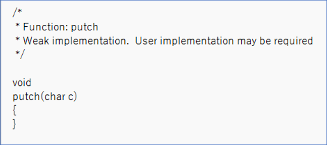
Since putch() is hardware-dependent, the user must implement it. A template
(skeleton) for putch() is included in a subfolder of the directory where
XC8 is installed. You copy this template into your own source file and
implement the necessary content. I pasted it into the source file for CNSL
Module (cnsl.c).
 |
 |
| Template of putch() |
Implmentation example of putch() (from the manual of XC8) |
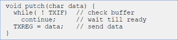
The example in the upper right cannot be adopted because it waits for the
transmit register to become empty. If you wait for an event like that,
the execution time of putch() becomes longer. As a result, printf() also
takes more time to complete, and the task that called printf() ends up
running longer as well. This undermines the system’s real-time responsiveness.
Inside putch(), all it should do is place the character to be sent into
the transmit FIFO buffer and enable the interrupt. The rest is left to
the UART driver.
The figure below shows the putch() routine used in the CC-218 FW. At the
beginning of the routine, there is a while() loop that waits for space
to become available in the transmit FIFO buffer. This was added as a precautionary
measure for least expected cases. Under normal conditions, this loop passes
through without iterating.
In the CC-218 FW, function names and variable names are defined based on Hungarian notation.
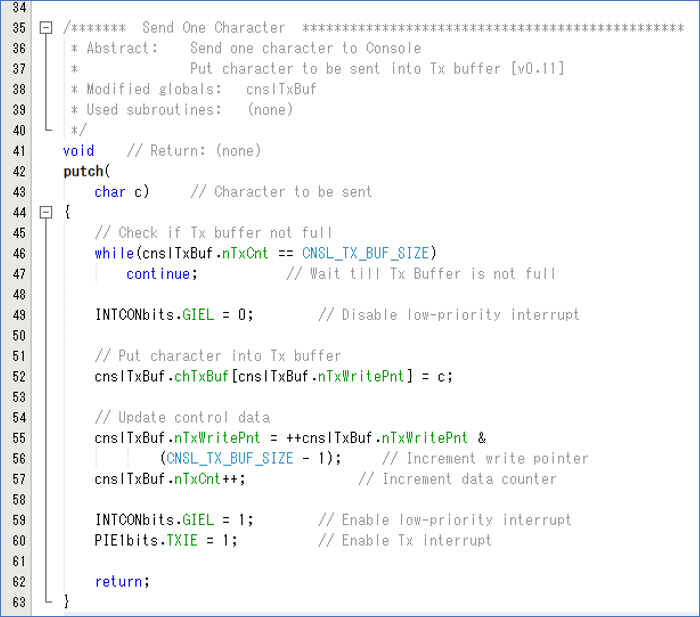 |
| Implementation ofputch() (CC-218 FW) |
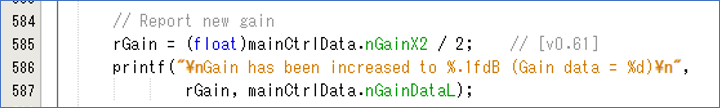 |
| Example of usage of printf() |
printf() is a very convenient function, but it consumes a lot of memory.
In the case of XC8, it uses about 11KB. Since the program memory of PIC18F2520
is 32KB, printf() alone takes up about one-third of it. If it's likely
to run out of memory, you’ll need to stop using printf() and create a simpler,
custom function instead.
In CC-218 FW, the program memory usage stayed within 86%, so printf() continues
to be used.
Tera Term has timestamp and logging features. Enabling both of these features and saving the log can be very useful later on.
 |
| Example of Tera Term log -- Opening message of CC-218 FW |
Specification of IR remote
I believe that among DYI amp builders, few have incorporated infrared remote controls. Though may not be necessary, I’d like to provide a brief explanation of the infrared remote control interface as well.
Japanese companies tend to be closed off, so the specifications for infrared
remote controls are not publicly disclosed. While searching for information,
I came across a certain document (Ref-42, pp.263~274) that provides an
overview of the specifications of Japanese infrared remote controls. It
mentioned the existence of a unified standard called the “Home Appliance
Association Format” and noted that companies like Vishay and NEC manufacture
IR receivers. For details on the reference, please see the page "References."
This book is old (from 2005) and I later found out that it doesn’t reflect
the current situation, it did make one thing clear: Vishay IR receivers
can be used.
After checking Vishay’s datasheet, I decided to use TSOP34838 (although,
as mentioned earlier, I should have chosen the improved version, TSOP34438,
instead). I planned to determine what kind of code was being used by examining
the output waveform of TSOP34838.
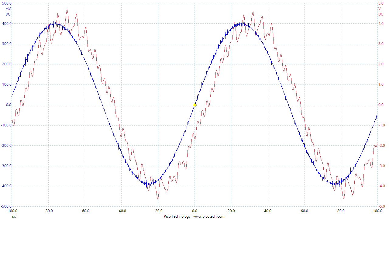
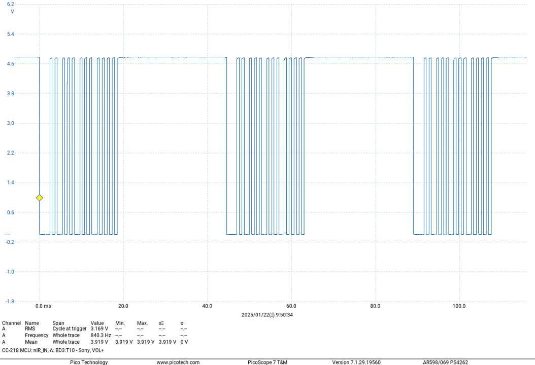 |
| Waveform of output signal of IR Receiver When VOL+ button of SONY RM-PZ3D is pushed |
Looking at this waveform, I was able to guess what kind of code was being
used.
I incorporated a routine into the firmware that converts this code into
numerical form and reports it to Console. The log below shows the codes
generated by pressing each button on IR Remote.
At first glance, the signal waveform appeared to be outputting 12-bit codes,
but upon closer inspection, I found that the upper 4 bits were always '0'.
Since the buttons could be identified using only the lower 8 bits, I configured
the routine to display only the lower 8 bits (1 byte).
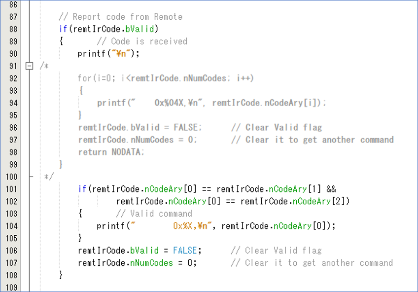 |
| Routine for displaying codes received from IR Remote on Console screen IR Remote Driver saves received codes into buffer (remtIrCode.nCodeAry), and sets the flag (remtIrCode.bValid). This routine sends the code to Console when the flag is set and three consecutive data in the buffer are the same code. |
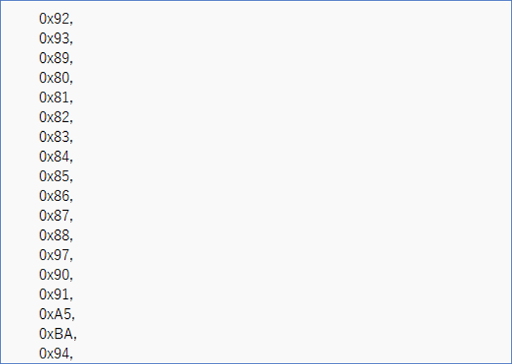 |
| Tera Term log -- Codes corresponding to each button on SONY RM-PZ3D Only this time, time stamp feature is disabled |
Copy the data from the log shown above and paste them into the source file
of the CC-218 FW (remt.c, specifically the remtGetCommand() function).
Then, edit them to turn it into an array of constants (see the figure below).
The received code is compared with this table (array) to identify which
button was pressed.
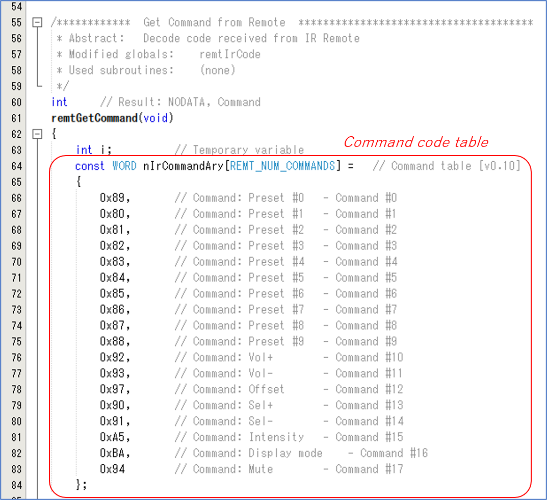 |
| Source code of CC-218 FW -- remtGetCommand() in remt.c Command code table created by editing the data copied and pasted from the log file |
Issues concerning PIC18F2520
There was no issue with the PIC18F2520 itself, but I was somewhat concerned
about the quality of its datasheet.
Personally, I’ve never found any errors—even spelling mistakes—in the datasheets
of major American semiconductor manufacturers like Texas Instruments or
Analog Devices. In contrast, Microchip (a UK-based manufacturer) frequently
has simple mistakes and ambiguous expressions in their datasheets. I’d
like to point out one particular issue that made me confused.
In the section "7.8 Using the Data EEPROM," it states (underlined section) that data in EEPROM which is not frequently rewritten needs to be refreshed, and such data should be stored in flash memory. However, in the "Note" section below that, it states something to the effect that data which is rarely rewritten does not need to be refreshed. These statements seem to contradict each other.
 |
| Excerpt fromthe datasheet of PIC18F2520 |
The true intent of this statement is as follows:
Due to the nature of EEPROM, writing to one address can affect other addresses
as well. For example, suppose you store two data, A and B, in EEPROM. If
you repeatedly rewrite B while leaving A untouched, A may become corrupted.
Looking at spec D124, it states a minimum of one million cycles. In other
words, if B is rewritten over a million times without ever rewriting A,
there is a risk that A may become corrupted.
What’s troubling about this explanation in the datasheet is that it seems to assume EEPROM will be used as a variable storage area. In the case of the PIC18F2520, EEPROM is located in a different address space from the data memory (RAM). To access EEPROM, you need to use special function registers (SFRs) such as EECON1, EECON2, EEDATA, and EEADR. At the very least, when coding in C, it is not feasible to use EEPROM as a variable area.
In CC-218 FW, the configuration data such as LED brightness and display mode are stored in EEPROM (which is presumably its intended purpose). The data is only rewritten when the user (myself) changes the settings. There’s no way it would be rewritten over a million times in my lifetime. Therefore, CC-218 FW does not perform any EEPROM refreshing.
Building
I carried out the processing and assembly according to the manuals.
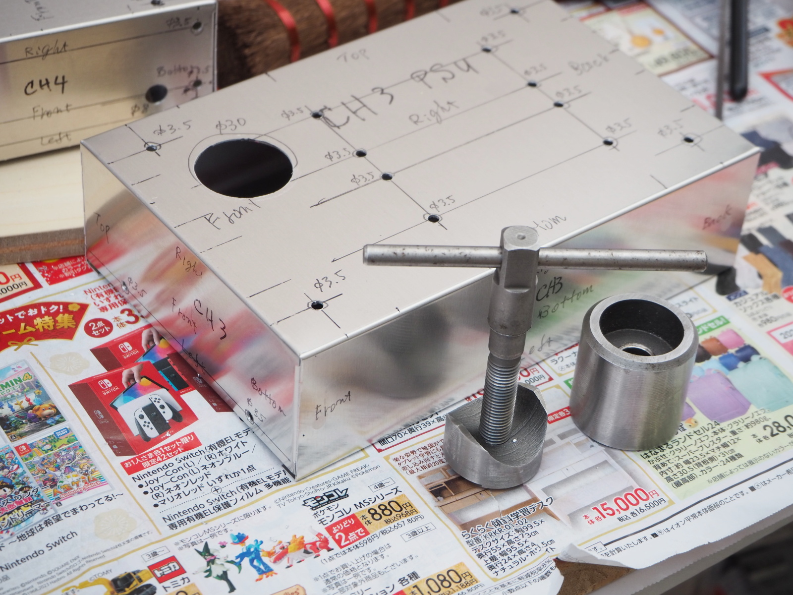
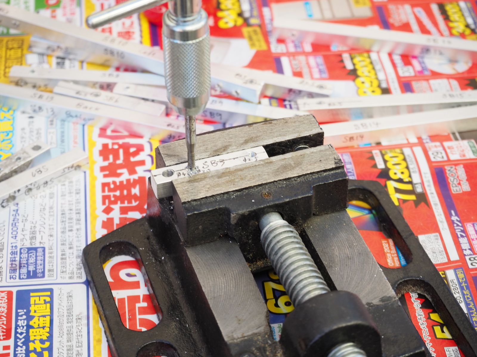
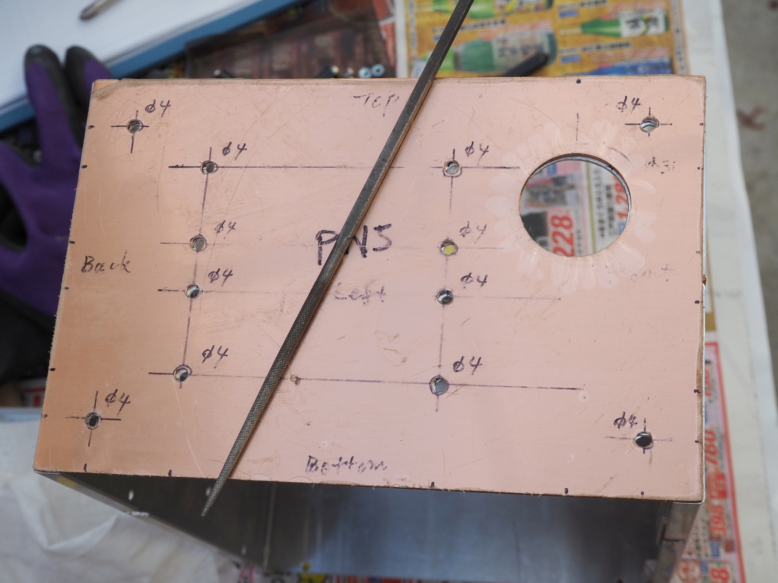
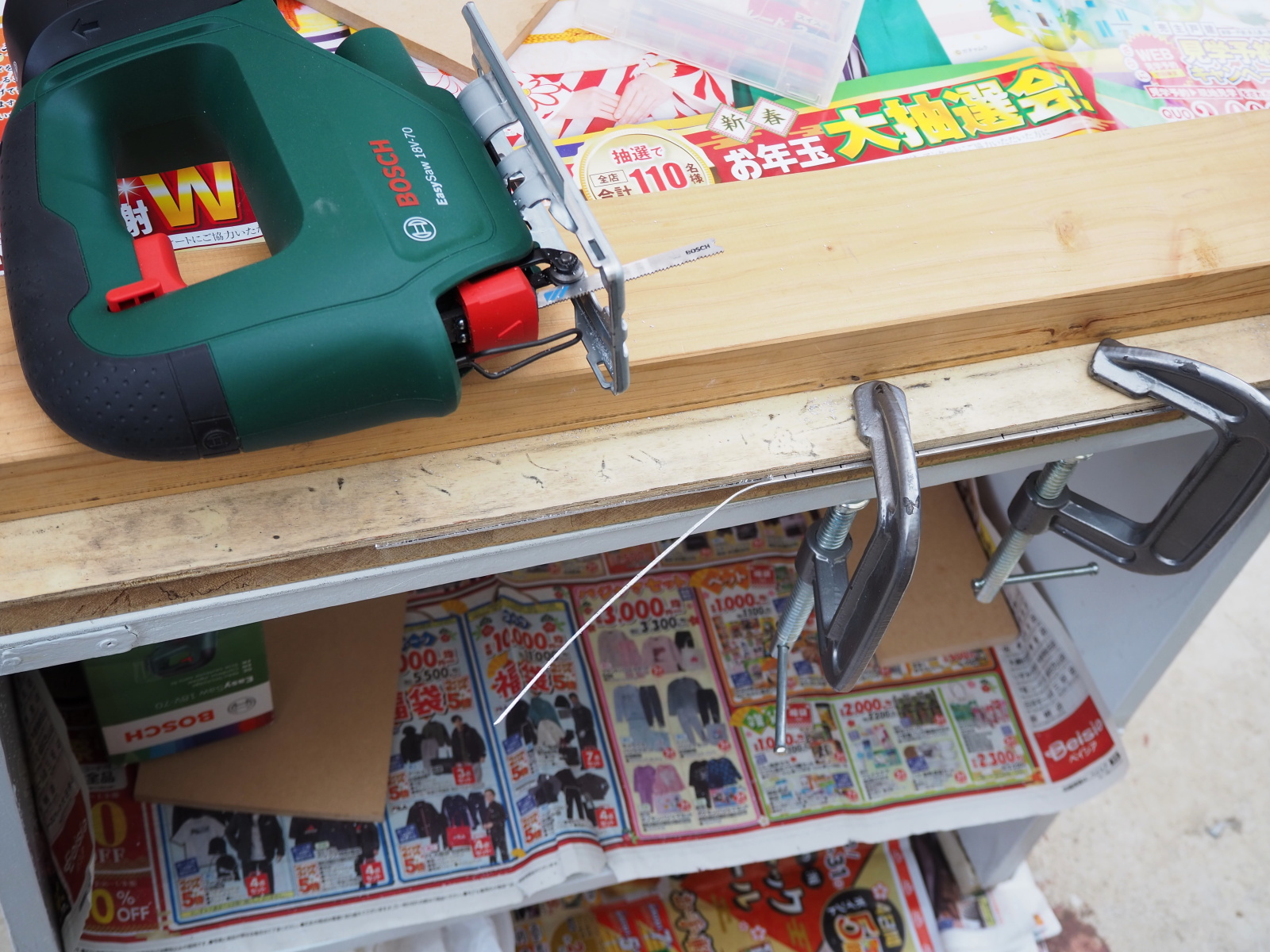
Metalwork
<Metalwork manual: CC-218_Metalwork.pdf>
 |
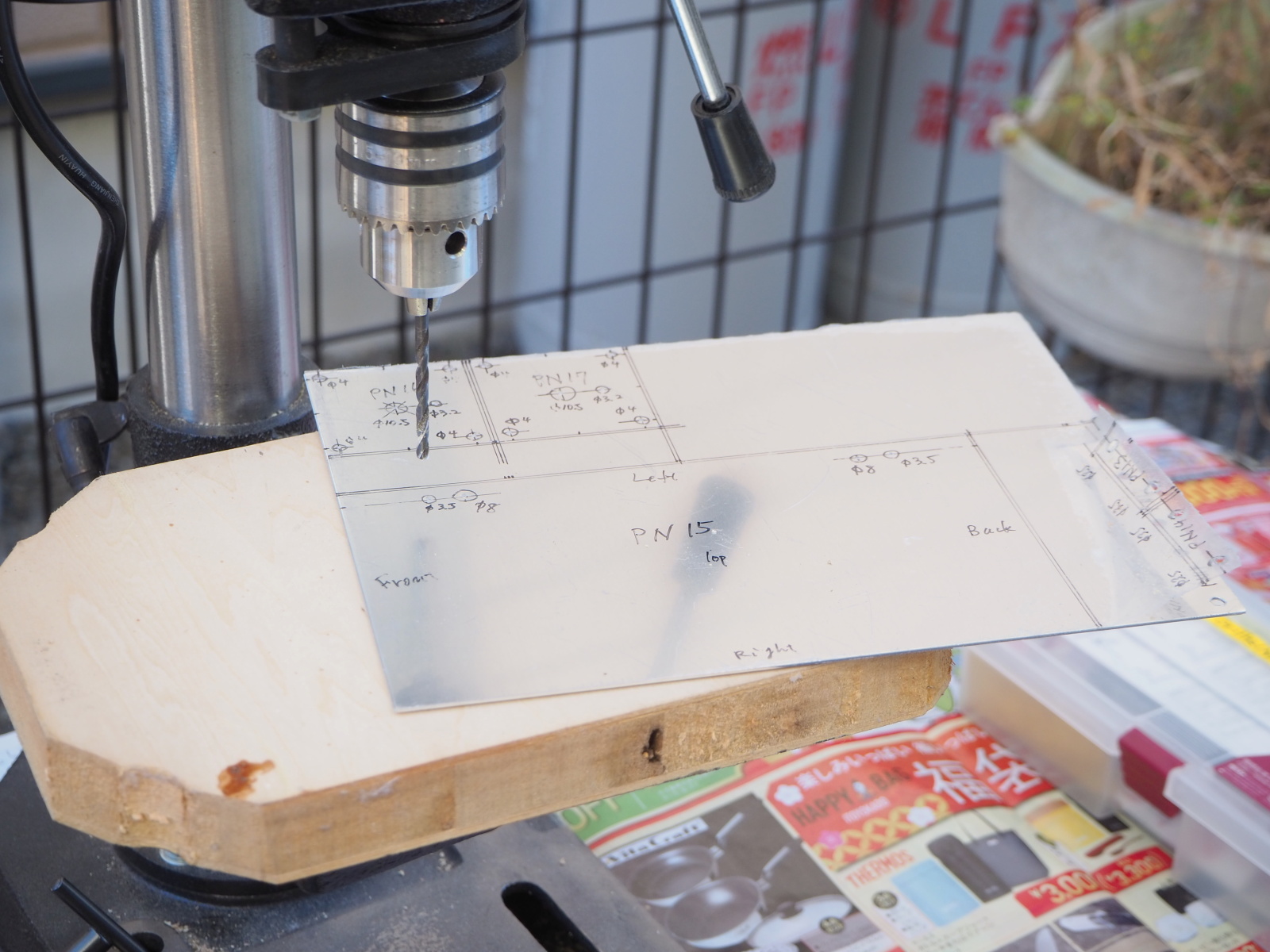 |
| Processing chassis |
Processing panels |
 |
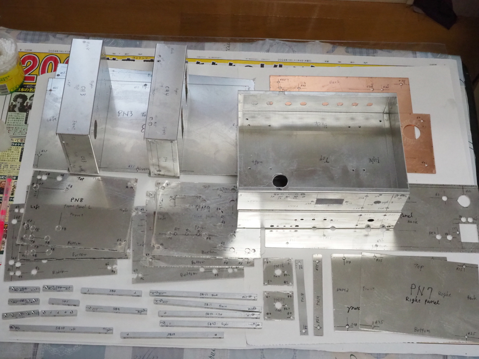 |
| Tapping the holes in bar nut | All the metal parts processed |
Processing Wood and plastic parts
<Manual for nonmetalic parts: CC-218_Woodwork.pdf>
 |
 |
| Processing knob Boring screw holes |
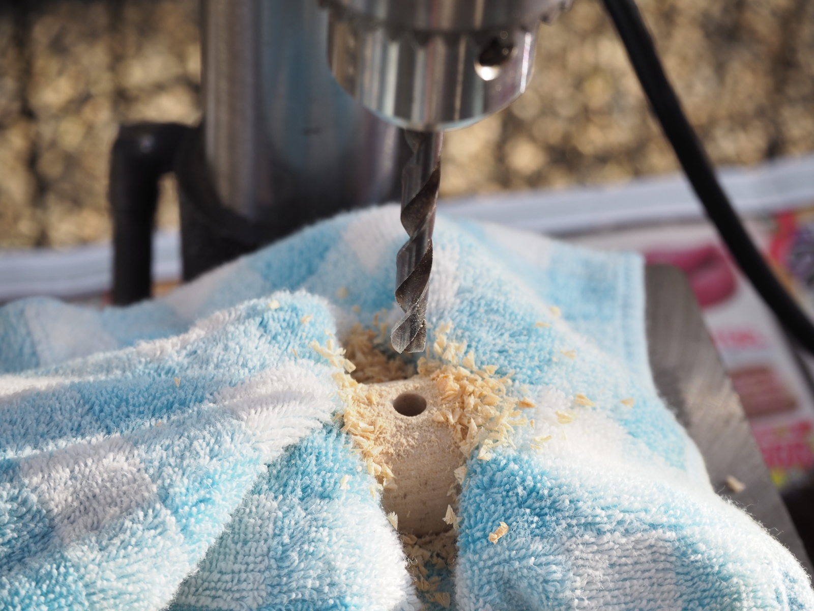
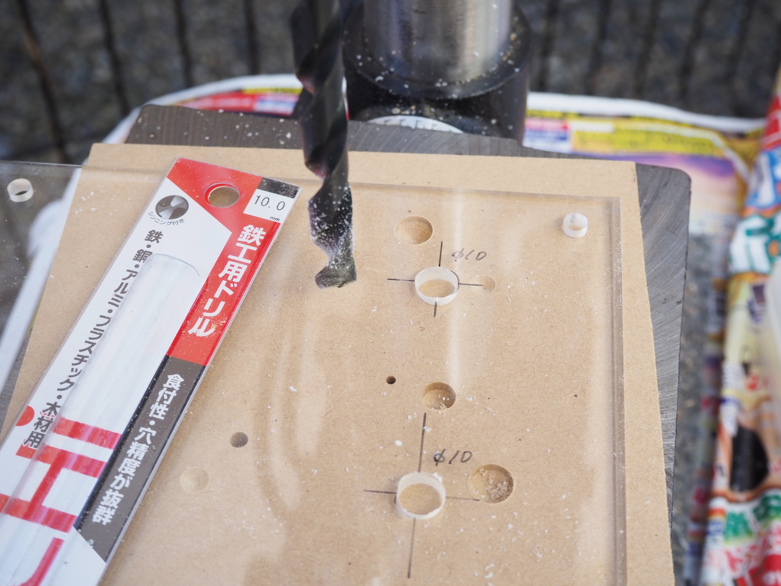
Processing acrylic panel Work carefully to avoid cracking the acrylic panel. Use drill bits of φ1.5, φ2.5, φ5, φ8, and φ10 mm to gradually enlarge the holes. |
Temporary Assembly
<Manual for temporary assembly: CC-218_PreAssy.pdf>
 |
 |
| Temporary assembly Correcting dimensional errors w/ files |
Temporary assembly The height of Back Panel was larger than the design by 1.5mm, so I cut it short w/ the power jigsaw |
 |
 |
| Temporary assembly Fitting Front Panels |
Temporary assembly Complete! (back view) |
Finish
<Finish manual: CC-218_Finish.pdf>
 |
 |
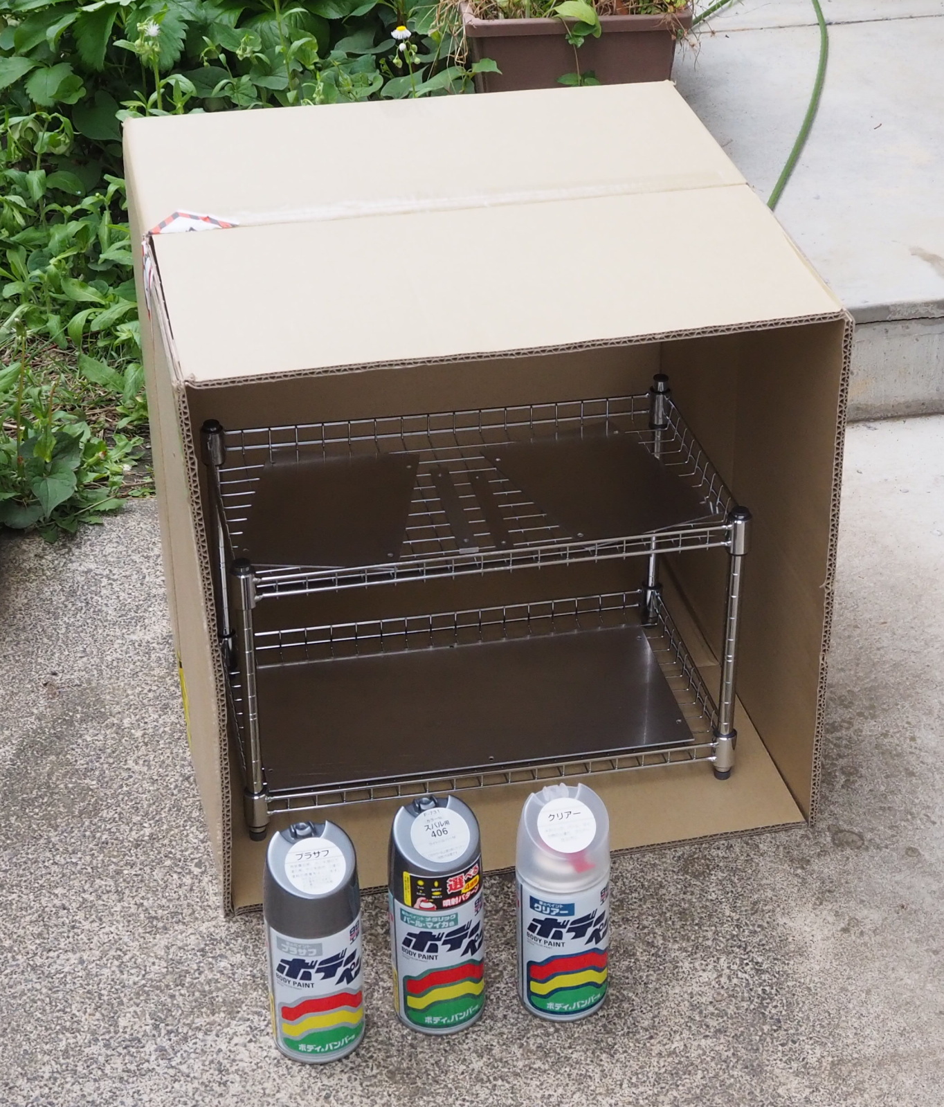
| Painting Painting Top Panel and Side Panels w/ silver metalic spray paint for automobiles |
Front Sticker (ST1) Cut out screw holes after printed w/ PC and printer |
Assembly
Assembly manual (total):
<Assy manual: CC-218_Assy.pdf>
Wire harnesses
<Wire harness assembly manual: CC-218_Design_WireAssy.pdf>
 |
 |
| Wire harness assy WH8 AnalogPower -- Under assembly |
Wire harness assy WH8 AnalogPower -- Complete! |
Modules
The assembly manuals for each module are included in the total assembly
manual.
<Assy manual: CC-218_Assy.pdf>
 |
| Assembly of modules VR Module (Left) and Rotary SW Module |
Boards
I employed PCBs for the first time in this project, and along with it,
the first time I used SMDs (Surface Mount Devices).
Among the SMDs, mounting the AS1115, which comes in a QSOP-24 package,
requires some skill. The QSOP has a pin pitch of 0.4mm, with only a 0.2mm
gap between pins.
A professional can solder it in no time using just a soldering iron. What's more, the result looks so clean, it’s as if it were done with reflow soldering. However, even without professional skills, it’s still manageable.
(1) Use a small amount of solder. Thin solder with a diameter of 0.5mm
or less is ideal (though I used 1 mm solder myself).
(2) Don’t worry if solder bridges form.
(3) Work quickly without lingering. Holding the iron tip on too long may
cause the pad to peel off.
(4) Remove solder bridges using solder wick (desoldering braid).
Although things should have gone smoothly following the steps above, my clumsiness got the better
of me—I ended up failing spectacularly. During the process, the IC shifted
out of position. Once soldered, you can’t remove it without using a special
tool. In the end, both the PCB and the AS1115 had to be scrapped.
Fortunately, I had spares for both the PCB and the IC, so I pulled myself
together and gave it another try. This time, it went well. When I checked
the connections with my DMM and confirmed that the soldering was well done,
I breathed a big sigh of relief.
<Assy manual for Display Board: CC-218_DISP_Assy.pdf>
 |
 |
 |
| Assembly of BD1:CC-218 DISP AS1115 (display controller chip) is mounted |
Assembly of BD1:CC-218 DISP Completed (top) |
Assembly of BD1:CC-218 DISP Completed (bottom) |
<Assy manual for Indicator Board: CC-218_IND_Assy.pdf>
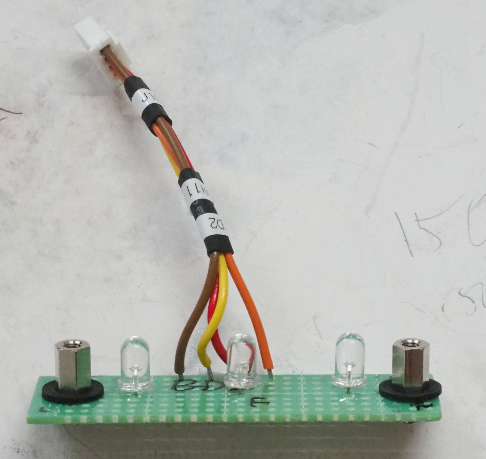 |
| Assembly of BD2:CC-218 IND Completed -- Wire harness (WH11) and screws are also mounted |
<Assy manual for Controller Board: CC-218_MCU_Assy.pdf>
 |
 |
| Assembly of BD3:CC-218 MCU Completed (top) |
Assembly of BD3:CC-218 MCU Completed (bottom) |
<Assy manual for Volume Board: CC-218_VOL_Assy.pdf>
 |
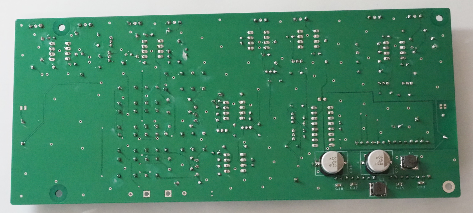 |
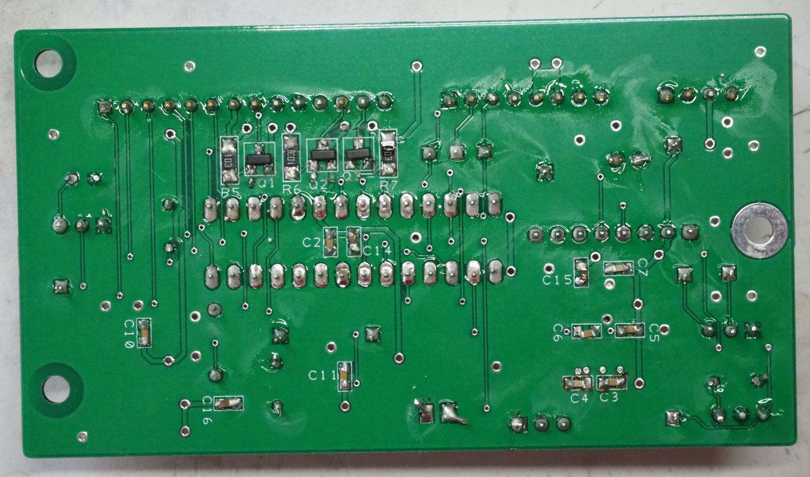
| Assembly of BD4:CC-218 VOL Rev.A Completed (top) |
Assembly of BD4:CC-218 VOL Rev.A Completed (bottom) |
<Assy manual for PhonoEQ Board: CC-218_EQ_Assy.pdf>
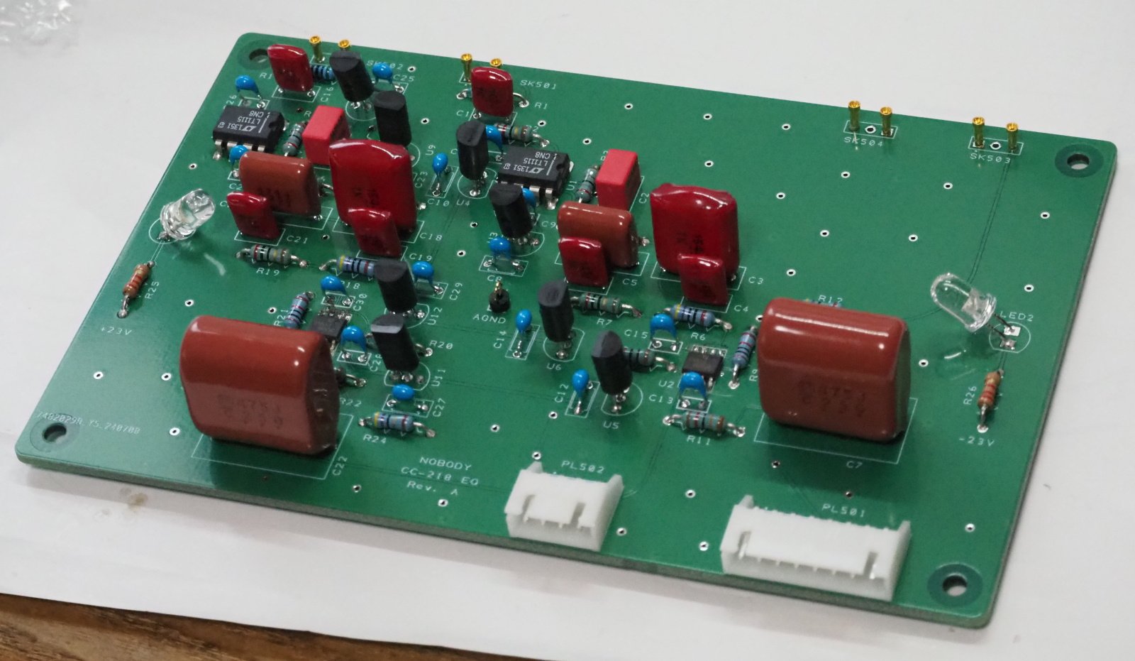 |
|
| Assembly of BD5:CC-218 EQ Completed (top) Hmm... 4.7uF capacitors are too big, aren't they? |
Assembly of BD5:CC-218 EQ Completed (bottom) There is one resistor mounted on the bottom, as it couldn’t be placed on the top due to a flaw in the PCB design. |
Total assembly
 |
 |
| Assembly of chassis The enclosure will never be disassembled, so the screws are fixed by bond |
Assembly of dirty compartment CH3:PSU |
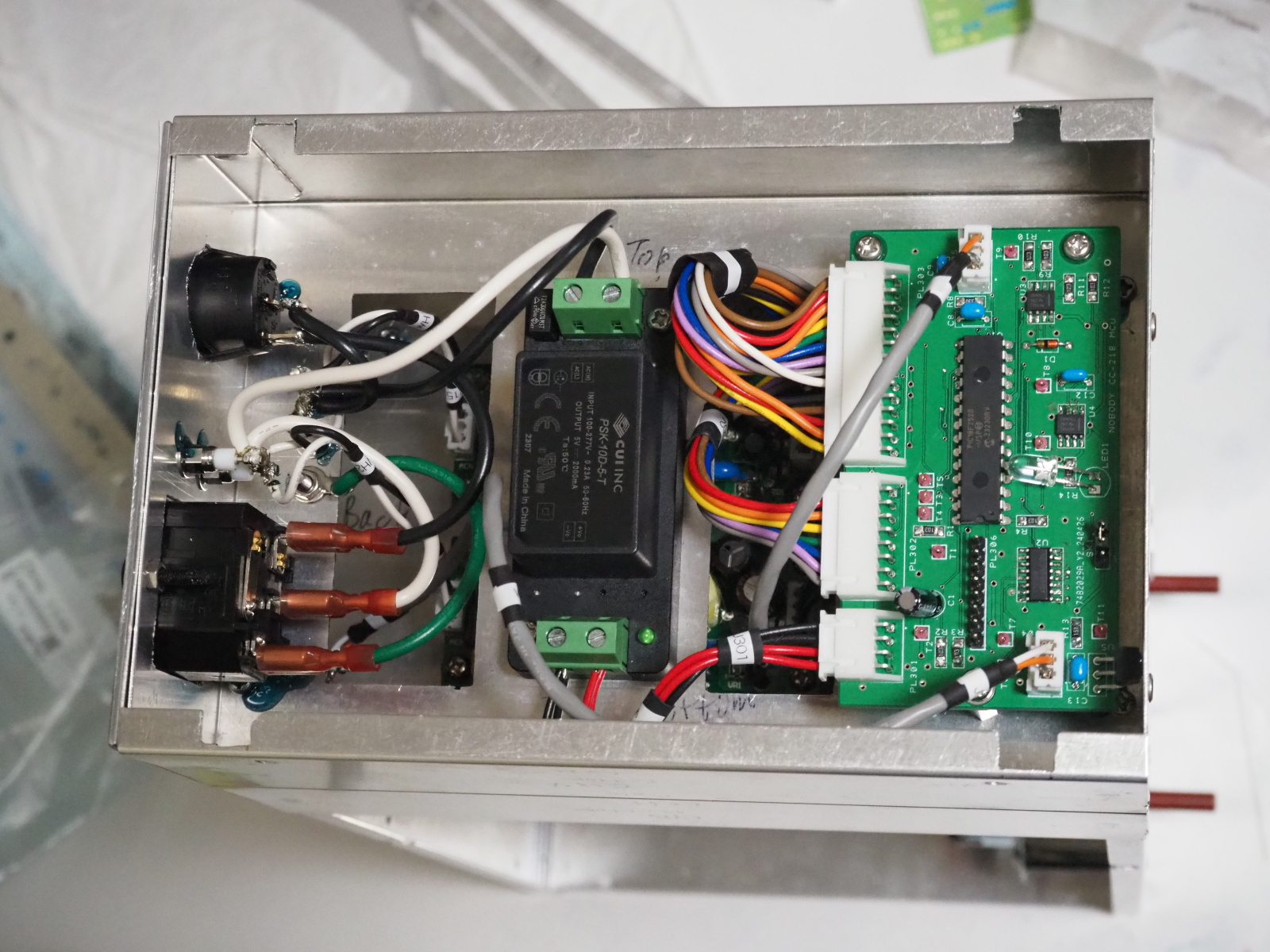 |
 |
| Assembly of dirty compartment CH4:MCU The AC/DC converter (PSK-10D-5-T) has been replaced by XP Power EML15US05-S because of the low performance of PSK-10D-5-T |
Fixing Back Panels |
 |
 |
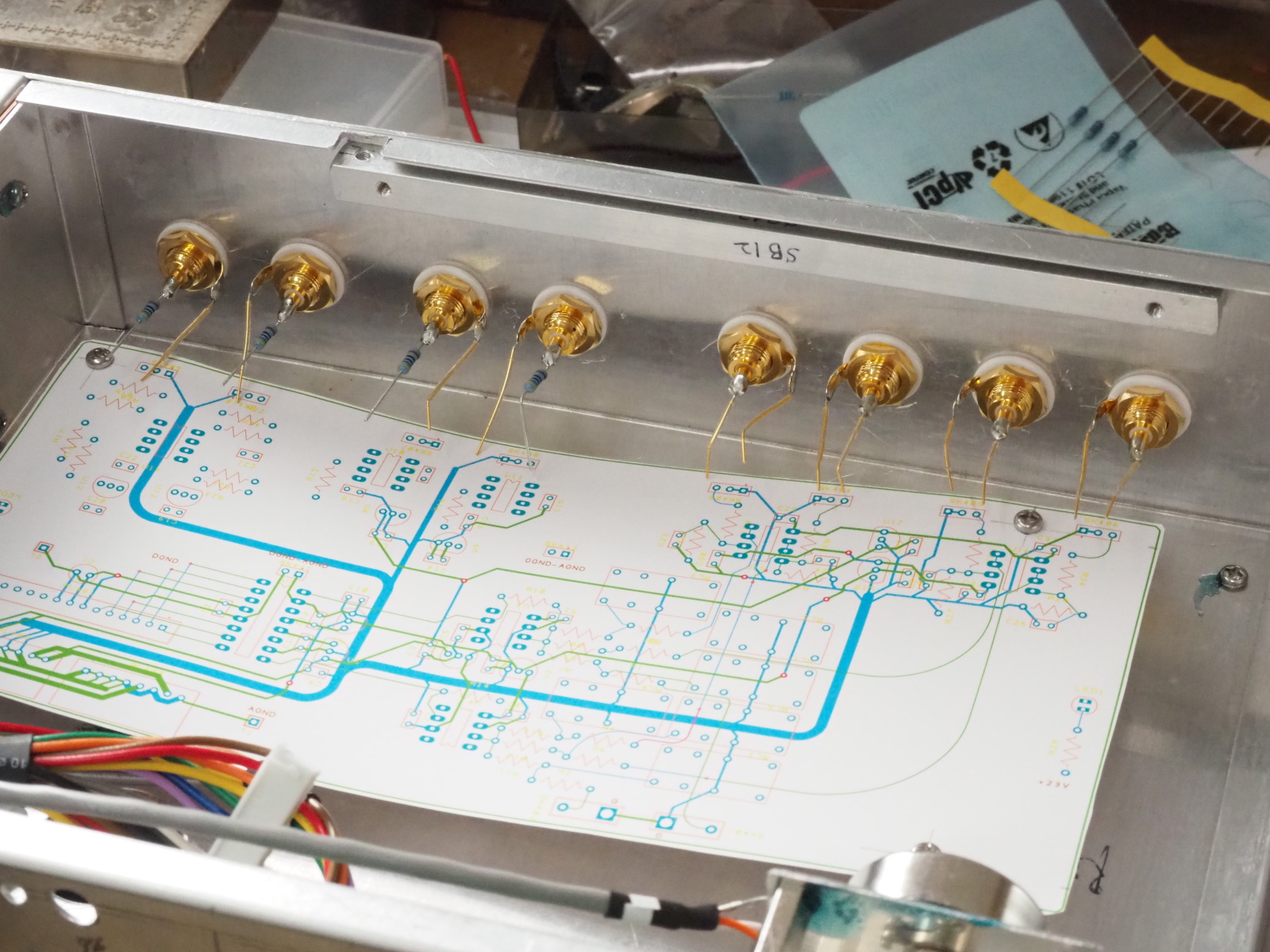
| Mounting RCA jacks CH1:AMP_VOL Soldering resistors (R1~4) and gold-plated OFC wires (W65~76) to the RCA jacks |
Assembly of clean compartment CH1:AMP_VOL Installing Volume Board (BD4:CC-218 VOL) Later, BD4 was improved to Rev.A, then to Rev.B |
 |
 |
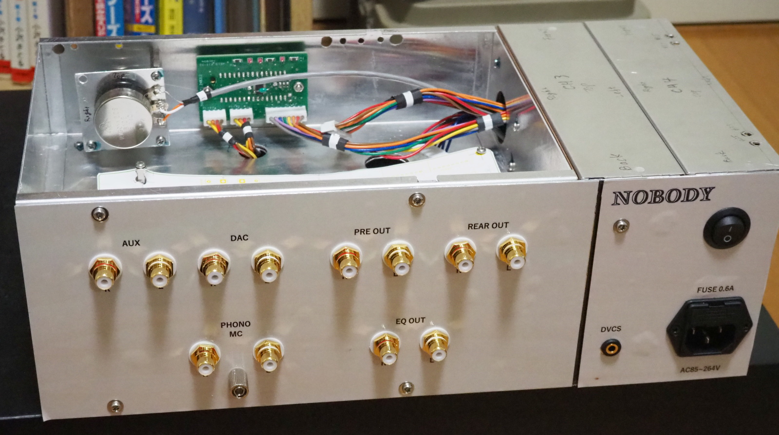
| Completed! Front |
Completed! Back |
Measurements and Improvements
Residual Noise
During the design stage, I was hoping for extremely low residual noise,
but reality wasn't so kind.
Even so, by implementing various countermeasures, I was able to reduce
the noise to a satisfactory level.
Shortcoming of AC/DC converter
For the analog power supply (±24V), I used the AC/DC converters for medical
devices. However, thinking that a regular one would suffice for the digital
power supply, I chose PSK-10D-5-T from CUI. This turned out to be a big
mistake. Measurements revealed that PSK-10D-5-T emits fairly strong electromagnetic
noise.
The figure below shows the waveform. Noise with peak values exceeding 5 mV
was captured. This includes not only noise superimposed on the signal lines
but also radiated noise picked up by the oscilloscope probe.
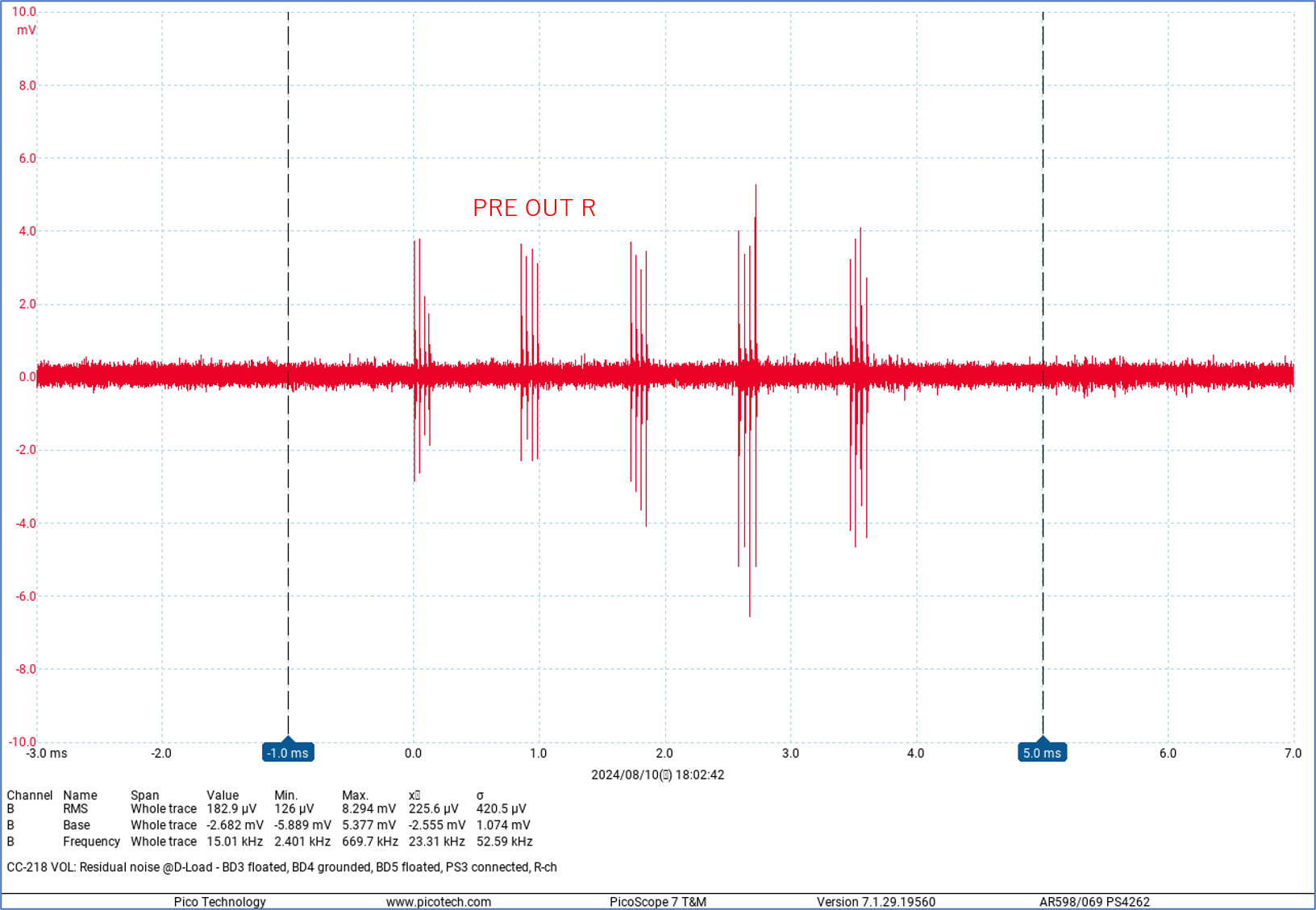 |
| Residual noise of CC-218 VOL -- 1st measurement PRE OUT R-ch Impulse noise occurs periodically |
I decided to replace the digital power supply's AC/DC converter with one designed for medical equipment as well. I chose the EML15US05-S from XP Power, the same model used for the analog power supply."
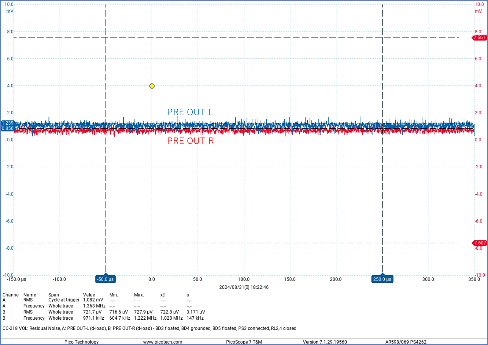 |
| Residual noise of CC-218 VOL -- After replacement of AC/DC converter PRE OUT R-ch RF noise in the range of 200kHz~1MHz is observed. The RMS value is approximately 130µV. |
SG-FG Connection
I experimented to see whether changing the SG-FG connection point would
affect the residual noise.
The output of Phono EQ Board (CC-218 EQ), which is more susceptible to
noise, was used for observation.
SG stands for Signal Ground. In the case of CC-218, this corresponds to AGND
(Analog Ground) and DGND (Digital Ground). However, on the schemetics of
the boards, AGND is sometimes simply labeled as GND. Similarly, on boards
consisting only of digital circuits, such as Controller Board (CC-218 MCU),
DGND is labeled as GND.
FG stands for Frame Ground, which refers to the potential of the metal parts
of the enclosure.
SG and FG need to be connected at some point in order to equalize their
potential. Once connected, the metal chassis functions as static shield.
In principle, a single SG-FG connection point is preferable. However, according
to what I've heard, commercial amplifiers typically connect them at multiple
points. So, I decided to experiment with multiple connection points on
CC-218 as well.
In traditional terminology, a single-point connection is referred to as
'1-point grounding,' while multiple connections are called 'multi-point
grounding.' Since this terminology is convenient, I will also refer to
them here as '1-point grounding' and 'multi-point grounding' (or 2-, 3-point
grouding).
Among the boards of CC-218, BD3 (CC-218 MCU) and BD4 (CC-218 VOL) have one of their screw holes designed as a thru-hole, connected to SG. Using metal screws creates an electrical connection to FG, while using plastic screws and plastic washers isolates them from FG. During the planning phase, I intended to include a pin socket for SG on BD5 (CC-218 EQ) to allow easy connection to the FG terminal on the back panel. However, I completely forgot about this during circuit design, so I soldered a gold-plated OFC wire to the GND track on BD5 to connect its GND (SG) to the FG terminal.
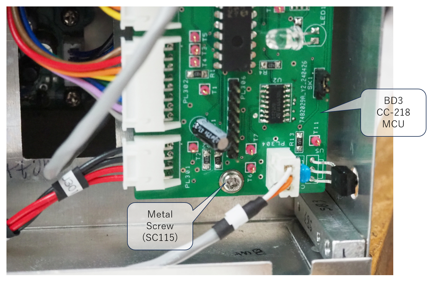 |
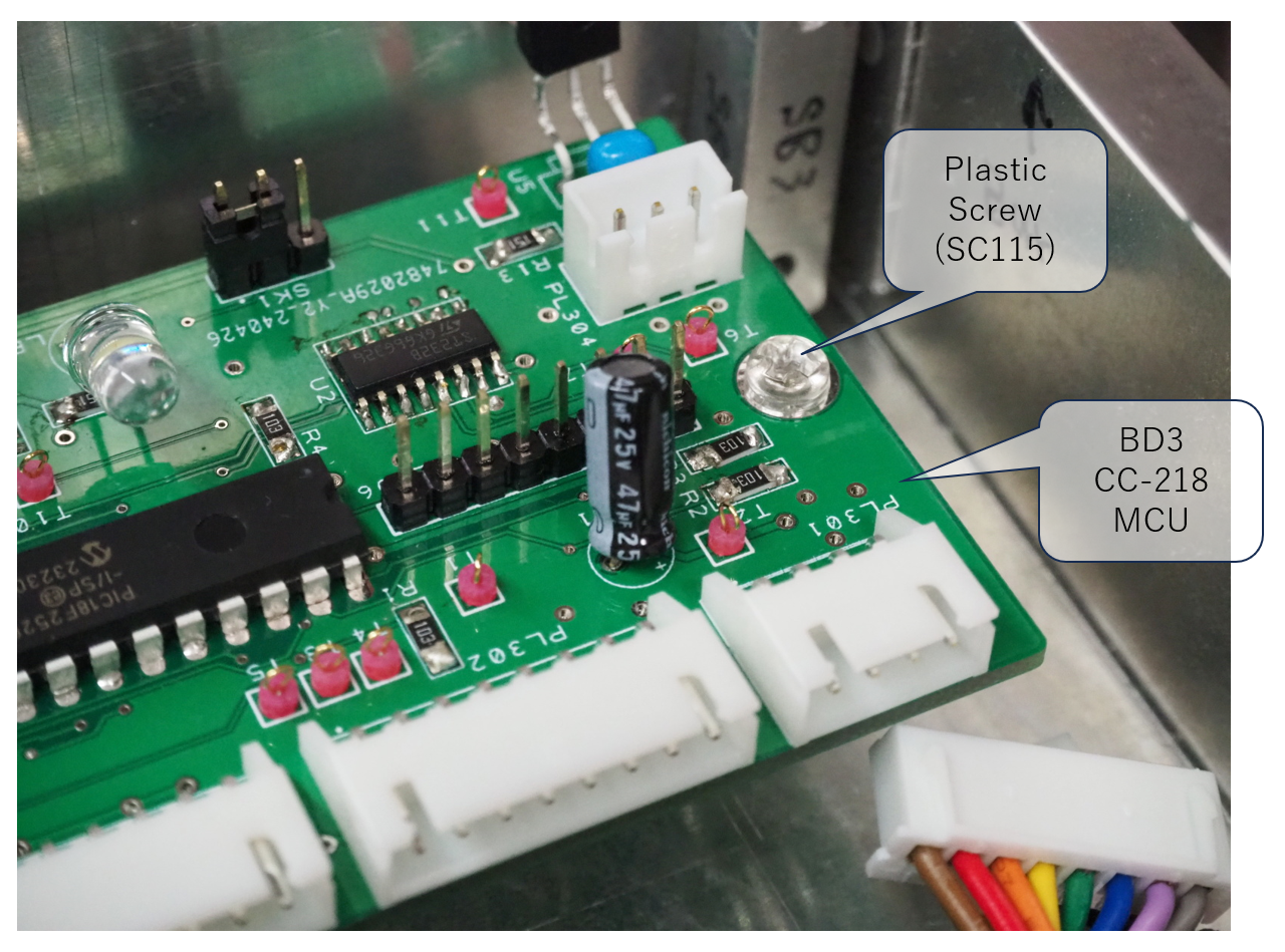 |
| BD3:CC-218 MCU -- SG-FG connected A metal screw is used for SC115 to connect SG to FG |
BD3:CC-218 MCU -- SG-FG unconnected A plastic screw is sued for SC115 to disconnect SG from FG |
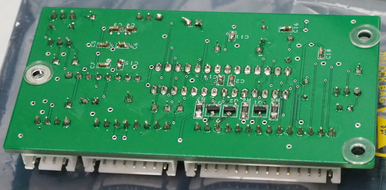 |
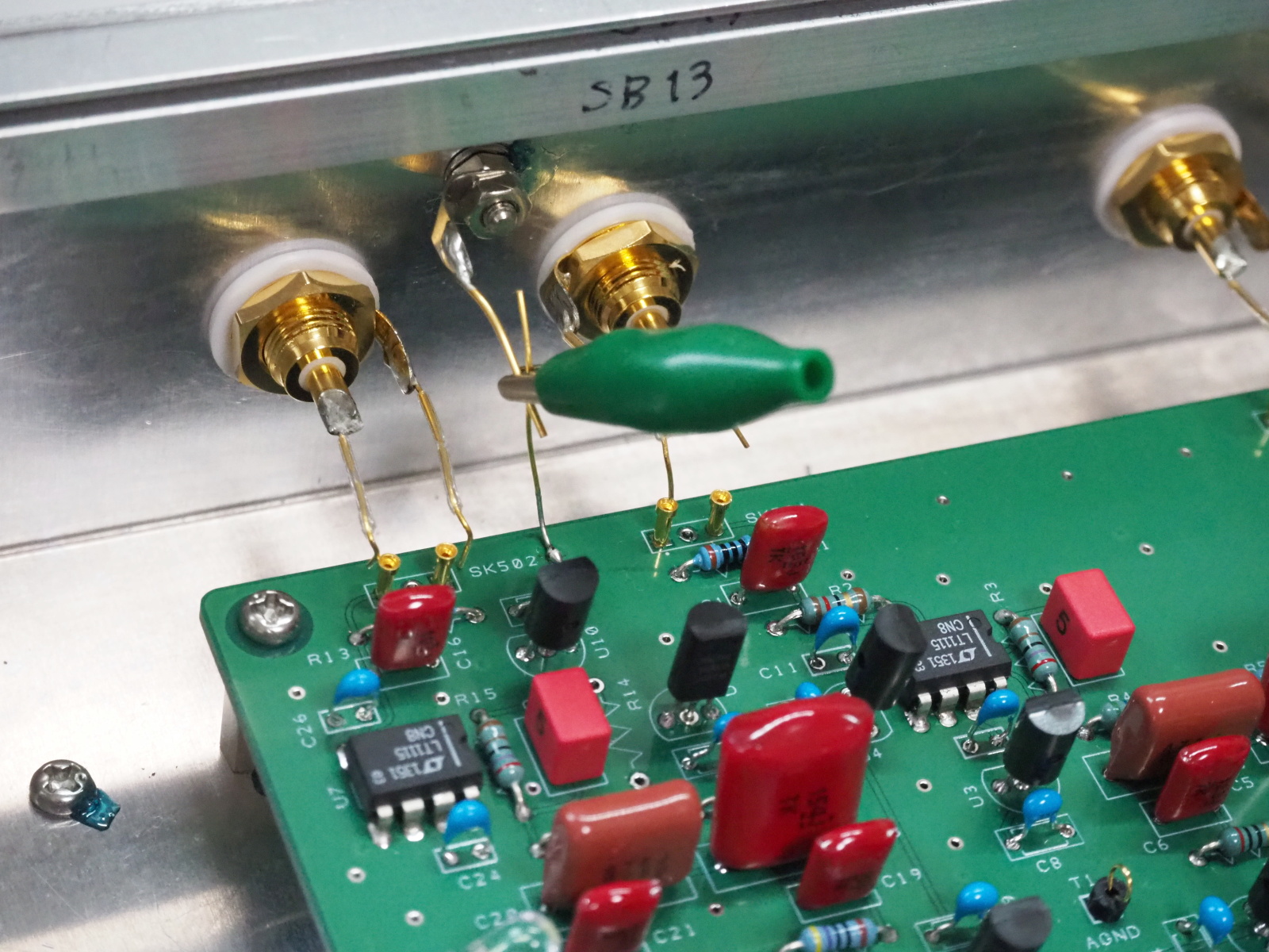 |
| BD3:CC-218 MCU -- SG-FG unconnected To isolate SG from FG, three plastic washers are also attached around the screw holes on the bottom side |
BD5:CC-218 EQ -- SG-FG connected SG and FG are connected via the gold-plated OFC wires |
I measured residual noise under the combinations of the grounding points shown in the table below.
| Condition | BD3 | BD4 | BD5 | EQ OUT L [uVrms] | EQ OUT R [uVrms] |
|---|---|---|---|---|---|
| 1-point grounding 1 | - | SG-FG | - | 684 | 622 |
| 1-point grounding2 | - | - | SG-FG | 637 | 552 |
| 2-point grounding | - | SG-FG | SG-FG | 646 | 629 |
| 3-point grounding | SG-FG | SG-FG | SG-FG | 713 | 681 |
When grounding is done only at BD5 (CC-218 EQ), the residual noise reaches
its lowest level. Since the measurement is taken at EQ OUT, this result
is expected.
Under the condition of 2-point grounding, the noise level does not decrease
compared to 1-point grounding.
Under the condition of 3-point grounding, the noise level actually increases.
This result supports the theory that DGND must be separated from AGND.
Since DGND is connected to AGND on BD4, under the condition of 3-point
grounding, both DGND and AGND currents coexist on FG (frame ground). And
this condition also creates loops.
I concluded '1-point grounding 1' is the best.
Although the numerical values were better with '1-point grounding 2', this
was because the measurement was taken at EQ OUT. Taking into account the
noise level at PRE OUT as well, I determined that grounding at BD4 was
the best option.
I don’t really understand the advantages of multi-point grounding.
As I interpret it, it may be effective when the chassis and/or circuit
board are too large to keep the internal SG impedance sufficiently low.
With multi-point grounding, SG and FG are connected in parallel, which
can reduce the impedance within GND.
Even if noise is picked up due to ground loops, the fluctuation in ground
potential may have a greater impact, so multi-point grounding could result
in better sound quality.
In the amplifiers I design, both the chassis and the boards are relatively
small, and because I use ground planes (described later), the SG impedance
is low enough that single-point grounding gives good results.
Since the noise level did not decrease even with multi-point grounding, I examined the waveforms to investigate the cause of the noise.
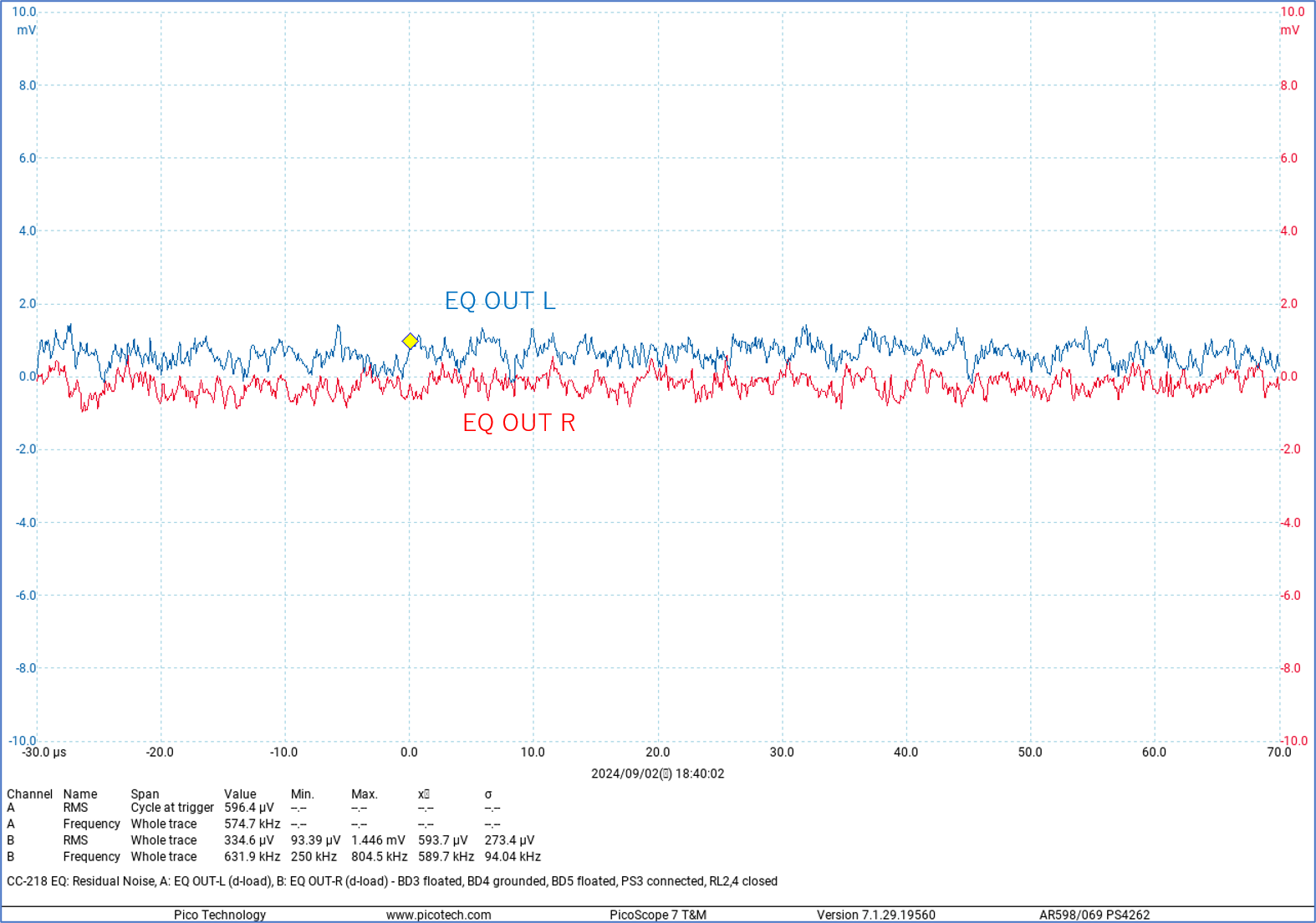 |
| Residual noise of CC-218 EQ -- 1-point grounding 1 EQ OUT L-ch, R-ch RF noise in the range of 250kHz~1.4MHz is observed |
As a result of the investigation, it was found that this RF noise was coming from the DC power rails. Though the AC/DC converters have a built-in line noise filter, the noise filter can only block high frequencies above 1 MHz. Noise below that frequency is not attenuated at all. Since it overlaps with the longwave and mediumwave bands, it is presumed that broadcast radio waves are being picked up.
Adding noise filter
Since I had already found similar noise in MV-217, I had initially planned to add a low-pass filter (LPF) on the secondary side of the analog DC power supply during the conceptual stage. However, I completely forgot about it when designing the circuit.
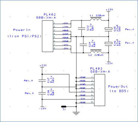 |
| Schematic (excerpt) of CC-218 VOL Rev.A Filter is added to DC power supply (+/-24V) from PL402 (Power In) LPF of fC=1.5kHz (L1~L2, C33~C38) |
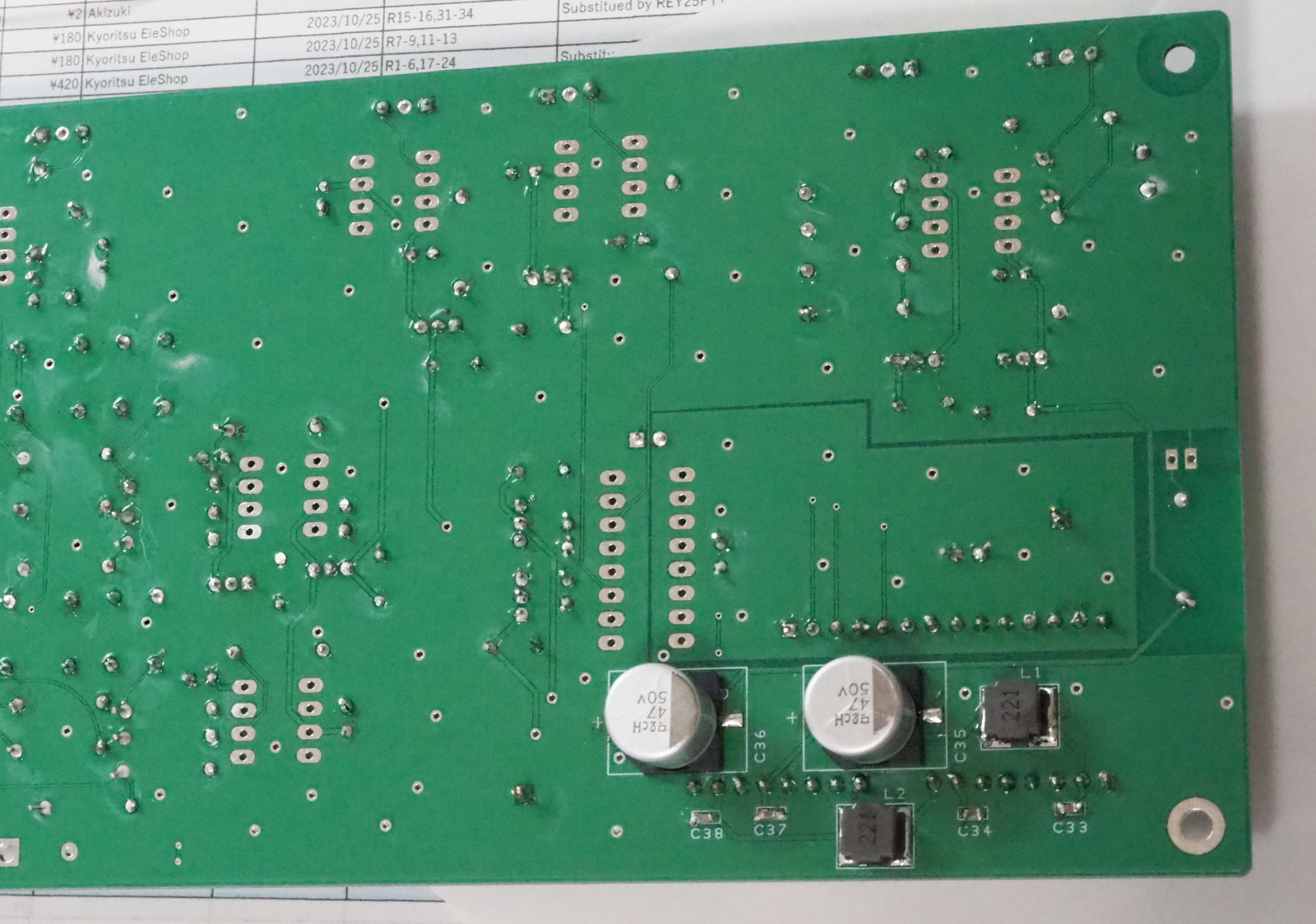 |
| CC-218 VOL Rev.A The LPF (L1~2, C33~38) is placed near PL402 (Power In) |
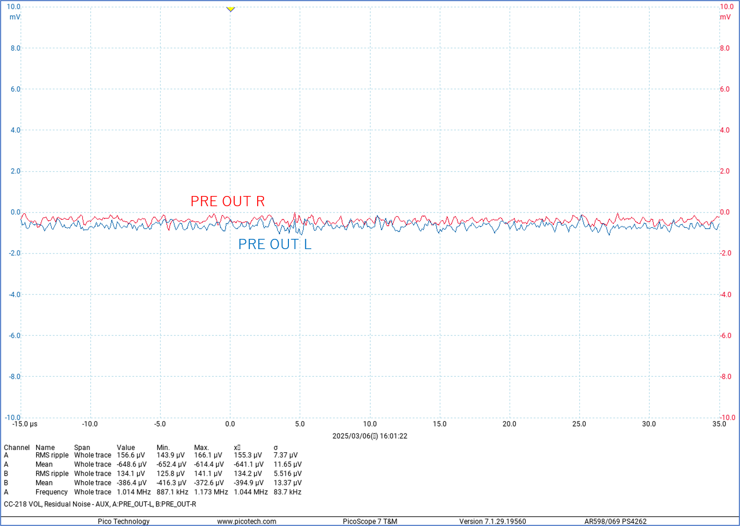 |
| Residual noise of CC-218 VOL Rev.A -- Noise filter added Noise below 1MHz is almost gone, but noise at 1MHz remains RMS value is the same as the level before the revision (about 130uV) |
GND plane
When adding the noise filter to the CC-218 VOL, I also changed the AGND
tracks to AGND planes. This is what’s commonly referred to as "copper
poured ground" or "ground plane." For DGND, using ground
plane is standard practice—if you don't, the signal waveforms become unstable
and can lead to malfunctions. The reason I didn’t initially use ground
plane for AGND was because my seniors had warned me that GND plane should
not be used in low-frequency amplification circuits.
As mentioned earlier ("PCB Design: PCB5"), after careful consideration, I adopted GND plane when designing the PCB for the CC-218 EQ (PCB5). The measurement results were excellent, so I decided to use GND plane for the CC-218 VOL Rev.A as well.
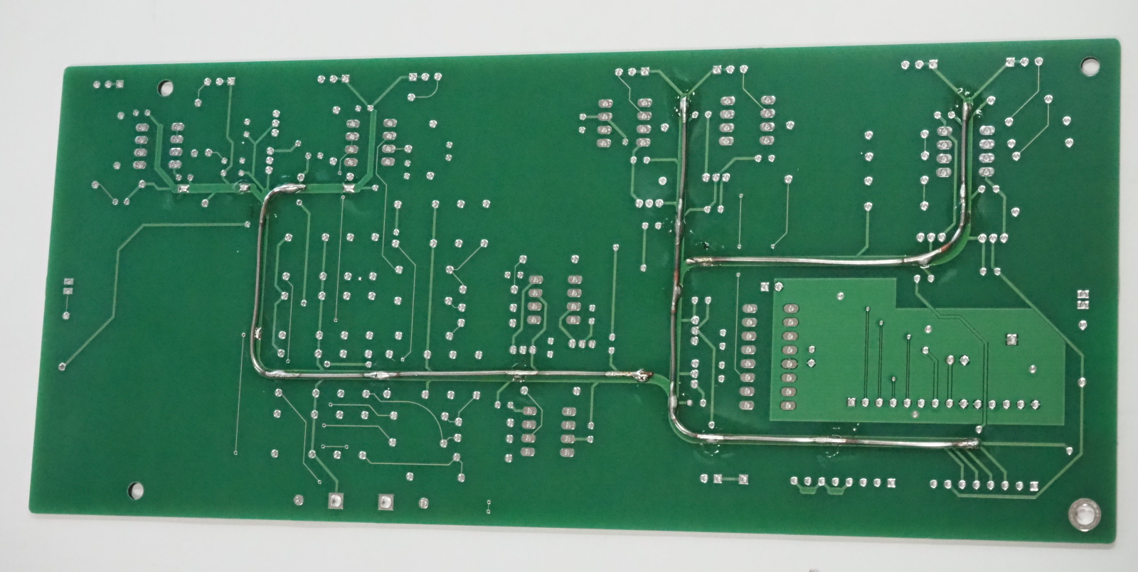 |
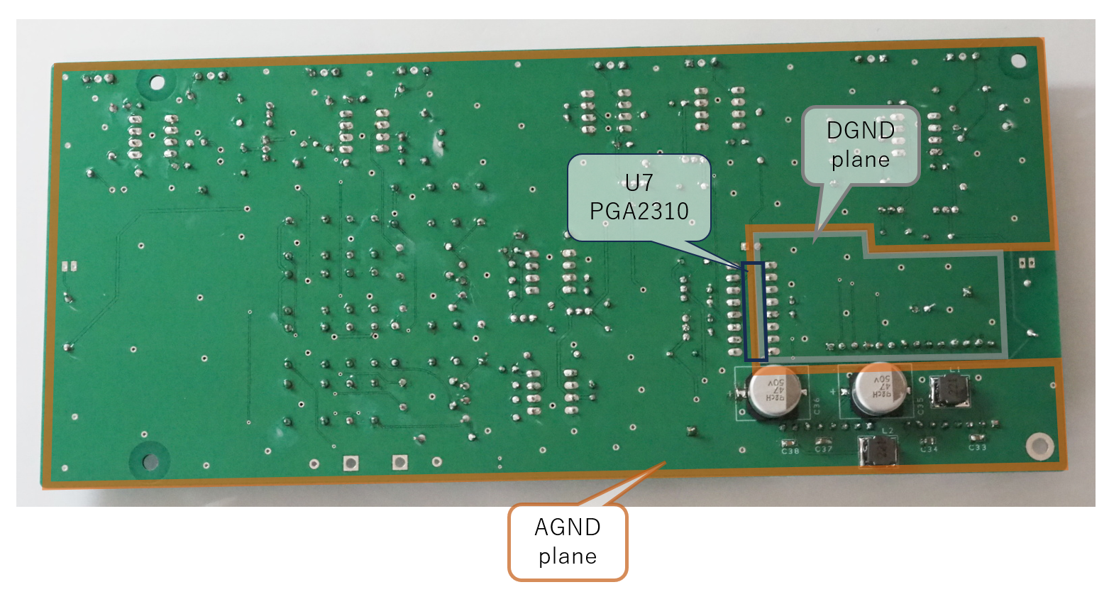 |
| Tracks of AGND of CC-218 VOL Ordinary tracks are used for AGND AGND tracks are reinforced by tin-plated copper wires to lower the impedance |
AGND plane of CC-218 VOL Rev.A Plane is adopted for AGND as well as DGND |
Additional revision to reduce noise
Even though the LPF was added to the DC power rails, noise around 1MHz
still remained.
Upon investigating the noise source, I found it was coming from the PGA2310—apparently
a clock component.
I decided to add LPFs to the output buffers of BD4. The schematic has been
revised to Rev.B. There was no need to modify the PCB design to implement
the filters. All I needed was to attach two resisitors to the PCB. So,the
PCB4 remains at Rev.A.
Two 1000 pF capacitors (C39~C40) are added between the input pins of the output buffers (BD4:U10(OPA627):P3, BD4:U11(OPA627):P3) and AGND. Since the two 1 k ohm resistors (R15~R16) had already been inserted in series near these input pins to prevent parasitic oscillation, the combination with the capacitors forms an LPF with fC=160 kHz (–3 dB). Though fC seems a little too low, these values were chosen to sufficiently attenuate the 1 MHz noise."
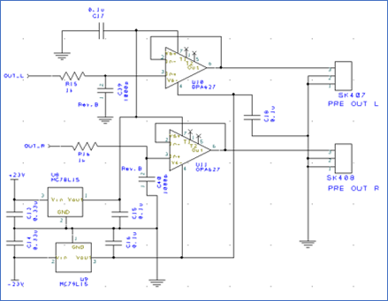 |
| CC-218 VOL Rev.B - Schematic (excerpt) 1000pF (C39~C40) are added to the input pins (P3) of the output buffers (U10~U11:OPA627) C39~C40 and R15~R16 (1k ohm) form LPF of fC=160kHz (-3dB) |
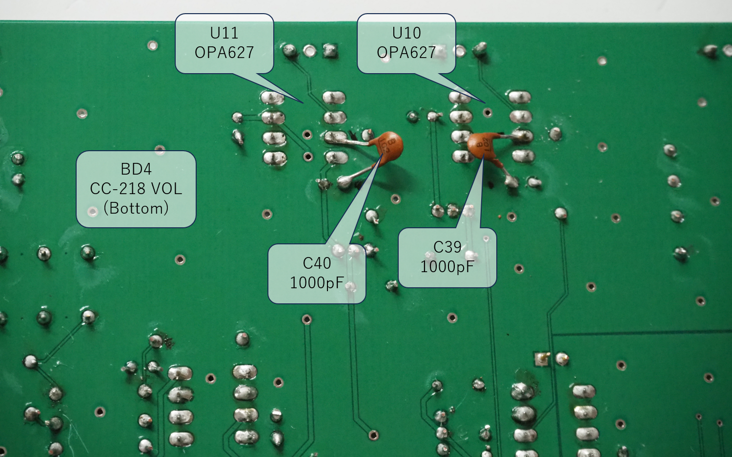 |
| CC-218 VOL Rev.B --Rework 1000pF (C39~C40) are soldered to U10:P3, U11:P3 |
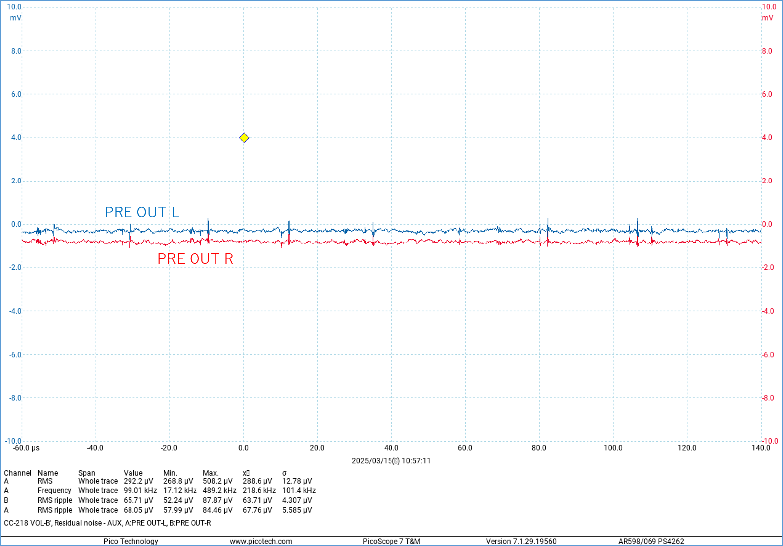 |
| CC-218 VOL Rev.B -- Residual noise Noise has been significantly reduced L-ch: 66uV、R-ch: 68uV |
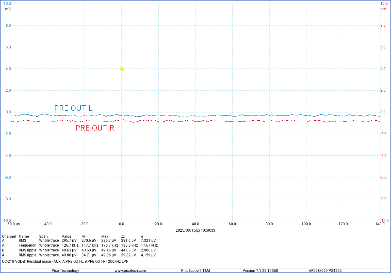 |
| CC-218 VOL Rev.B -- Residual noise (using oscilloscope's 200kHz LPF) L-ch: 50uV、R-ch: 41uV Fairly good waveforms. But I regard the data not using oscilloscope's LPF as the proper one, because I believe RF noise is a fatal drawback for preamps |
After many twists and turns, I could reduce the noise to the negligible level.
Another Kind of Noise
I discovered some concerning noise.
When the gain is changed, pulse-like noise occurs. The level is low, and
when the CC-218 is connected to either DIY Audio ACA V1.6 or dbx VENU360,
the noise is not audible. However, in the case of the TEAC AP-505, a popping
noise can be heard.
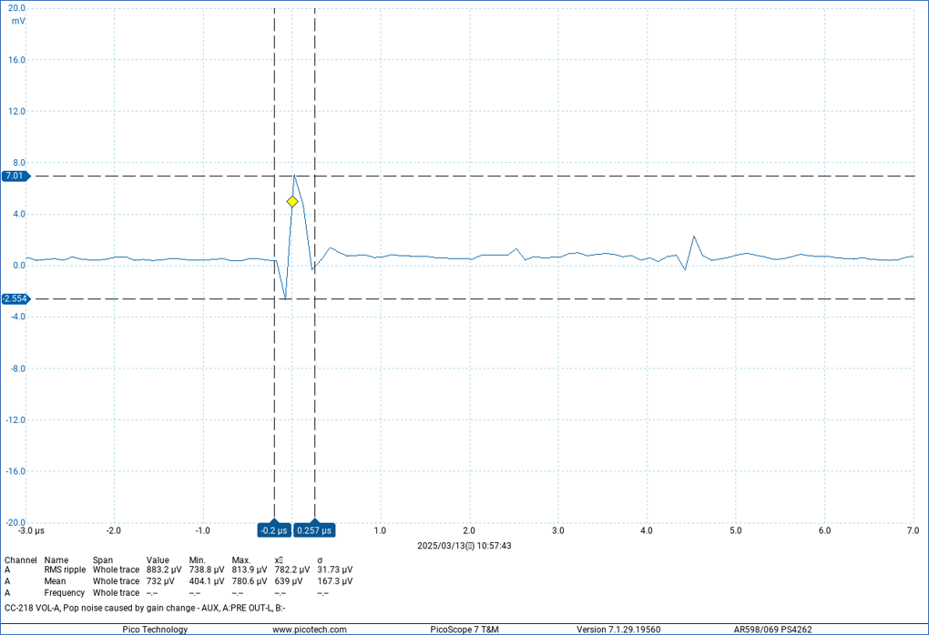 |
| Pop noise of CC-218 VOL Rev.A -- When the gain changes Waveform at PRE OUT Pulse width: less than 0.5usec, peak-to-peak: less than 10mV The noise has been reduced on Rev.B to the level to which the oscilloscope could hardly be triggered Nevertheless, AP-505 makes the noise audible |
The only possible cause of this noise is the electronic volume chip, PGA2310.
By adding the LPFs to the output buffers in the CC-218 Rev.B, I was able
to suppress the noise to some extent. However, to completely eliminate
it, higher-order LPFs are necessary.
Crosstalk
In this circuit design, a shunt-type selector was used, so I was concerned
about crosstalk between sources. Simulations showed that a worst-case crosstalk
of -94 dB could be achieved, so I set out to verify that.
Additionally, since I used the ICs (PGA2310, LME49720) that handle signals
of both left and right channels, I also measured the crosstalk between
channels.
Crosstalk between sources
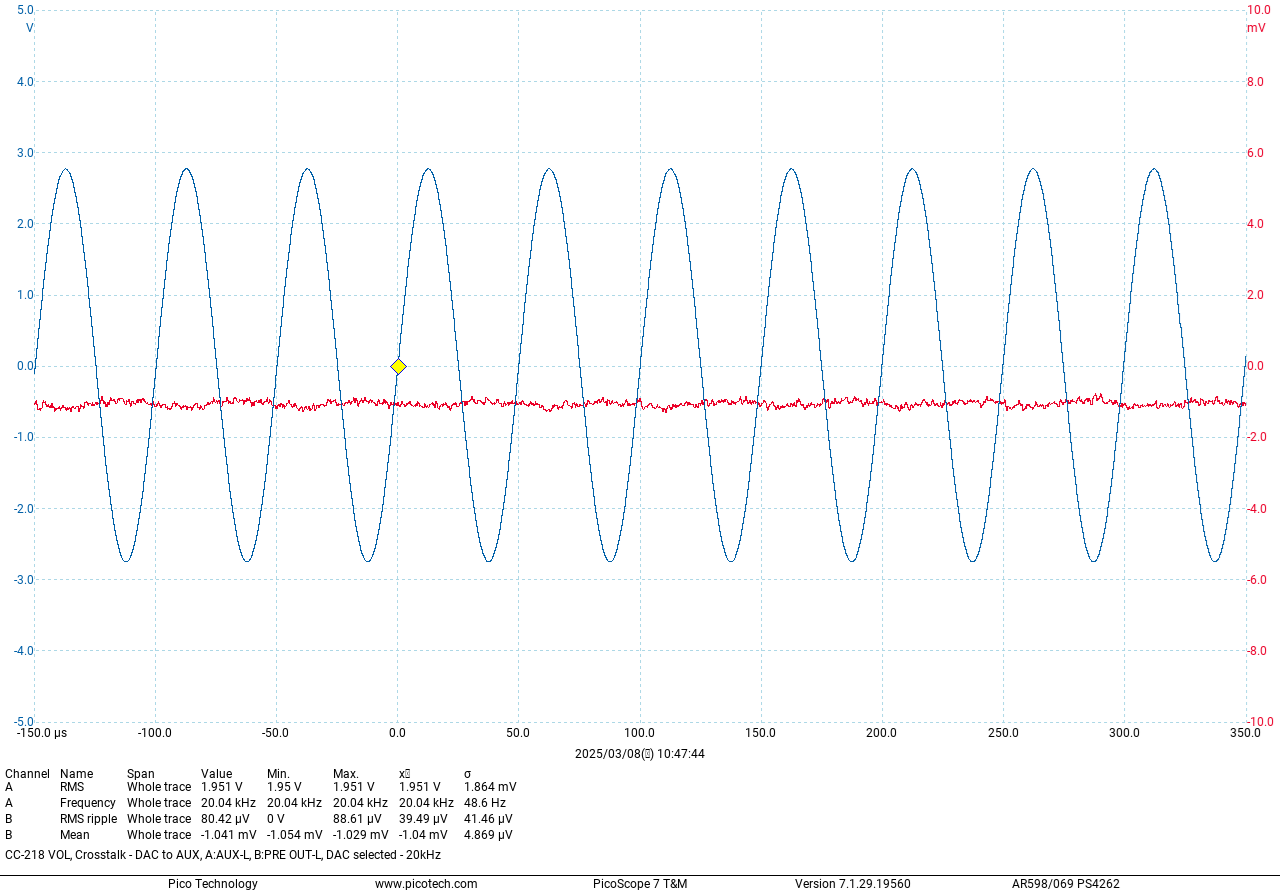 |
| Crosstalk of CC-218 VOL Rev.A --Between sources at 20kHz Blue: Input (AUX), Red: Output (PRE OUT), DAC is selected by Selector Low-level RF noise can be seen since CC-218 Rev.A doesn't have the output LPFs Component of 20kHz is observed, but its level is as low as -90dB or less |
Since the crosstalk is below -90 dB, I consider it to be acceptable.
If the contact resistance of the relays (BD4:RL1~RL6) increases over time
due to aging, crosstalk may increase.
However, the micro relays used in PA-210 showed no measurable increase
in contact resistance even after 20 years of use, as measured with a DMM.
The mini relays used in CC-218 are expected to experience even less aging,
so I believe they will be able to maintain their current performance for
the next 25 years.
Crosstalk between channels
The following figures show square wave response at 100Hz, 1kHz and 10kHz.
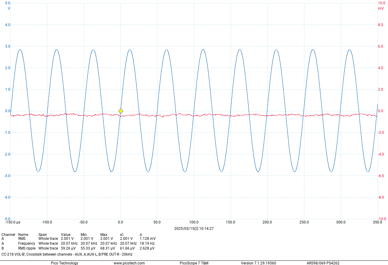 |
| Crosstalk of CC-218 VOL Rev.B -- Between channels at 20kHz Blue: Input (AUX-L), Red: Output (PRE OUT-R) Component of 20kHz is observed, but its level is as low as -90dB or less |
The result was similar to that of the inter-source crosstalk.
I conclude that there is no issue.
Charisteristics in Frequency Domain
Frequency response
Thanks to the GND planes, the frequency response remained flat even in
RF range.
Without the input/output filters, the response for the LINE input attenuates
only about -1.2 dB even at 1MHz.
In older NOBODY amplifiers, peaks often appeared around 200k ~ 400kHz,
but CC-218 exhibits none of that instability. I believe this result comes
from the stable ground potential and the absence of signal crosstalks which
are provided by the GND planes.
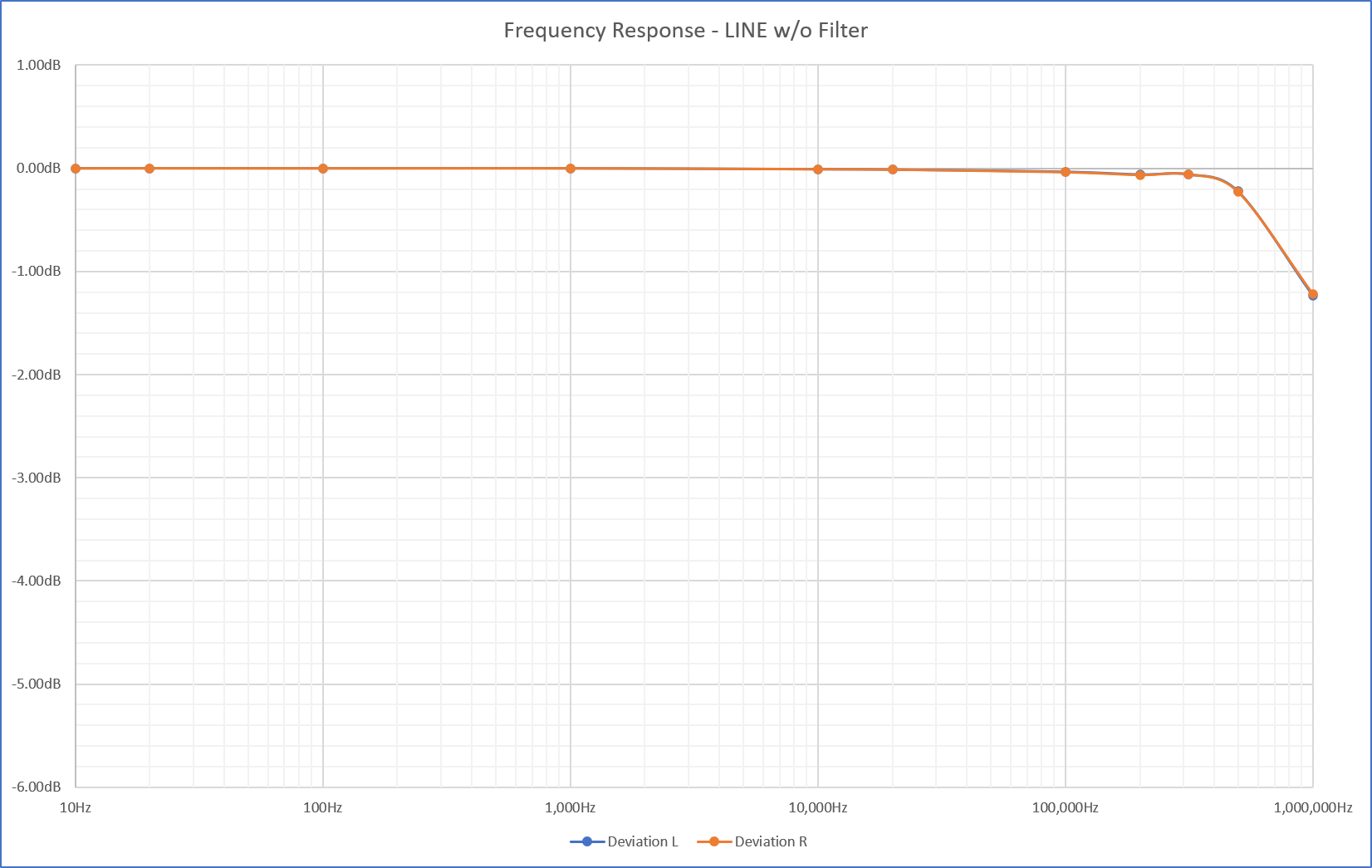 |
| Frequency response of CC-218 -- LINE input, w/o filters Input: AUX, Output: PRE OUT fC (-1dB): approx. 800kHz |
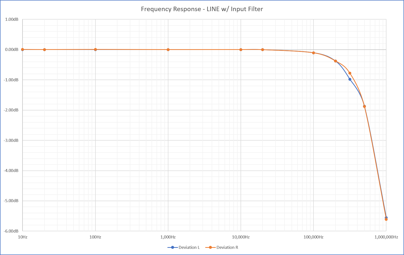 |
| Frequency response of CC-218 -- LINE input, w/ input filters Input: DAC, Output: PRE OUT fC (-1dB): approx. 400kHz |
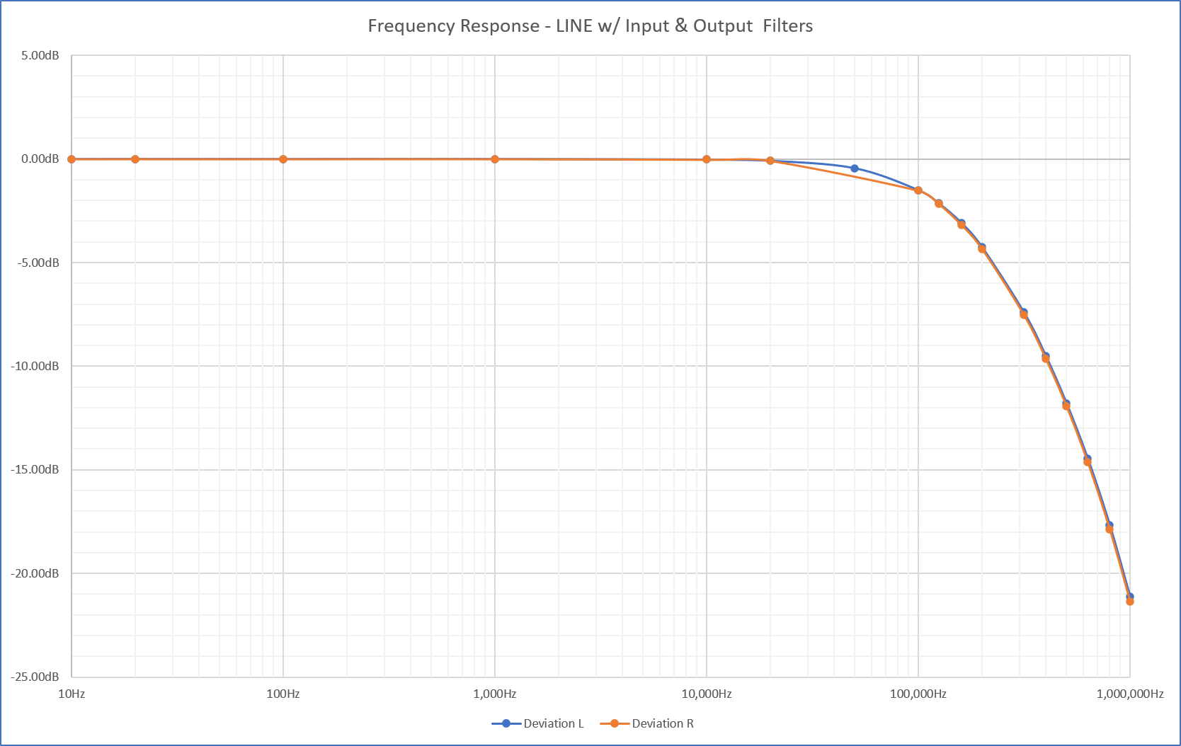 |
| Frequency response of CC-218 -- LINE input, w/ input & output filters Input: DAC, Output: PRE OUT fC (-1dB): approx. 70kHz |
RIAA Deviation
The RIAA deviation of the phono EQ closely matched the simulation result
and turned out well.
It mostly stays within the target range of ±0.1 dB (though it slightly
exceeds that at20 Hz on R-ch).
Though the graph appears to slope upward, that's because the vertical axis
is magnified; the difference between 20Hz and 10kHz is only about 0.15dB,
which can be considered flat.
The channel deviation falls within the range of -0.02dB to +0.05dB. Channel deviation affects sound quality even more than RIAA deviation (as it can impair soundstage reproduction), but in this case, the value is sufficiently low.
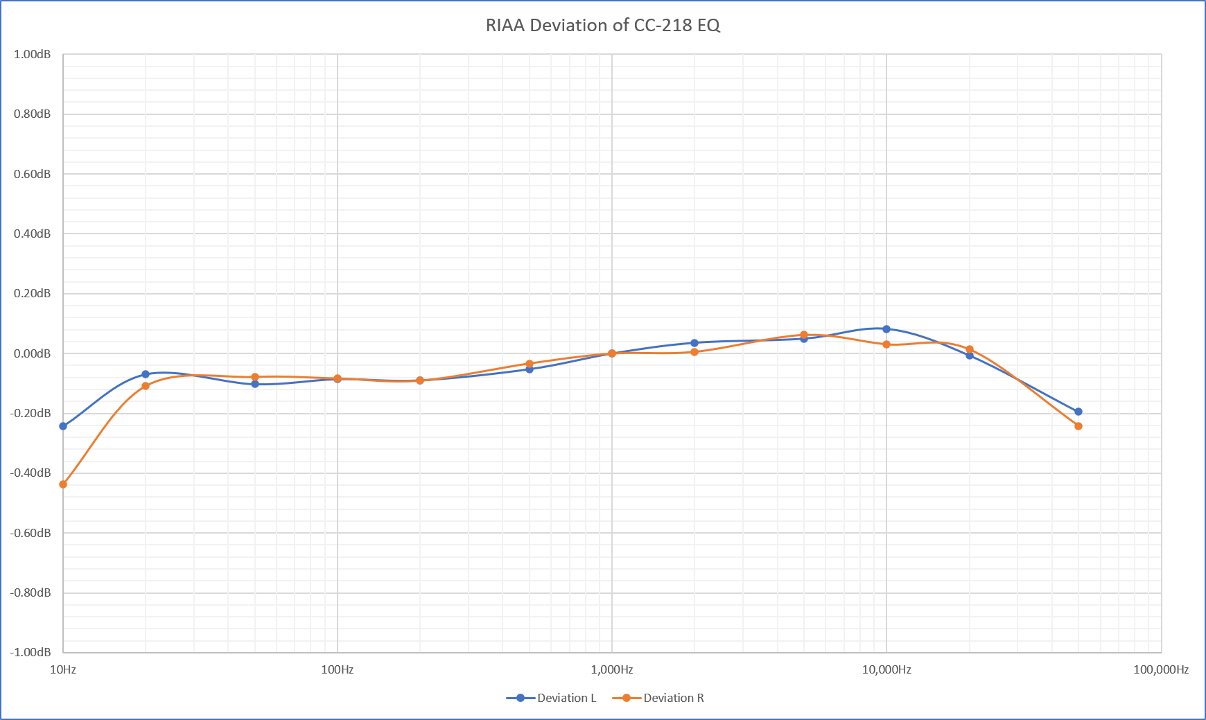 |
| CC-218 EQ -- RIAA deviation Input: PHONO, Output: EQ OUT RIAA deviation (20~20kHz): L-ch: -0.10dB(@50Hz) ~ +0.08dB(@10kHz) R-ch: -0.11dB(@20Hz) ~ +0.06dB(@5kHz) Channel deviation (20~20kHz): -0.02dB(@50Hz, 500Hz, 20kHz) ~ +0.05dB(@10kHz) |
There was nothing in CC-218 EQ that required modification.
Gang error
Once I adopted the eVolume chip PGA2310, there was no longer any need to
worry about gang error, but I measured it just to be sure.
In the figures below, “Target Gain” refers to the gain set on PGA2310.
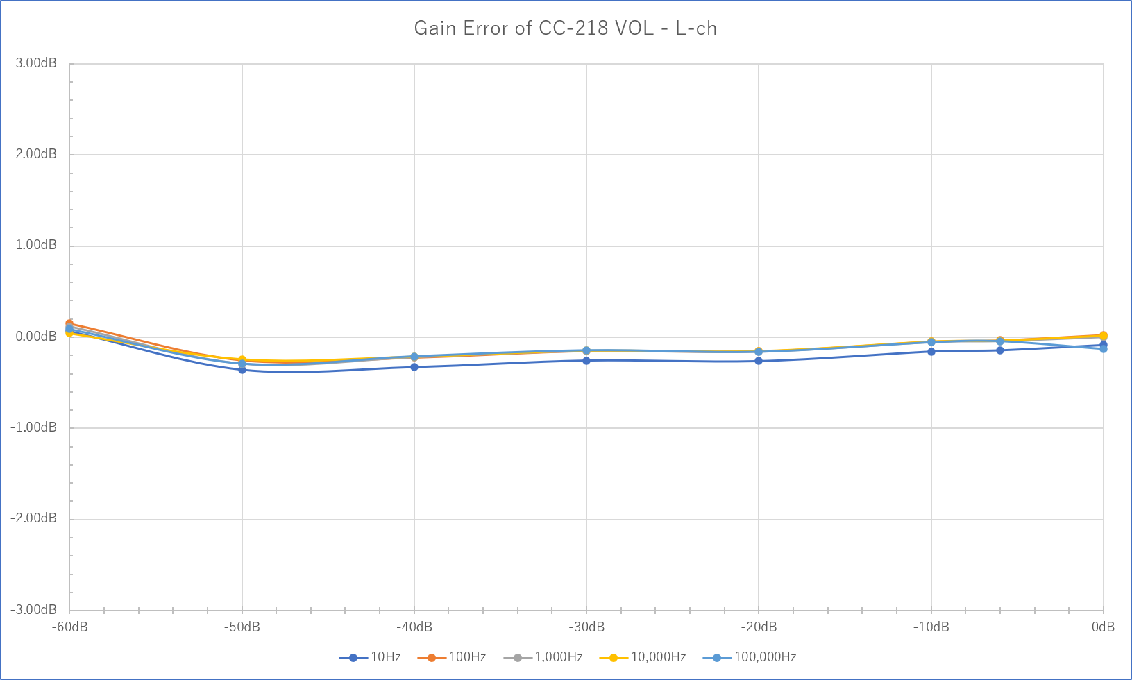 |
| CC-218 VOL gain deviation -- L-ch Input: DAC, Output: PRE OUT The graph shows the difference between the target gain (horizontal axis) and the measured gain (vertical axis). The gain is extremely close to the target values at all frequencies (deviation: -0.3dB to +0.15dB). |
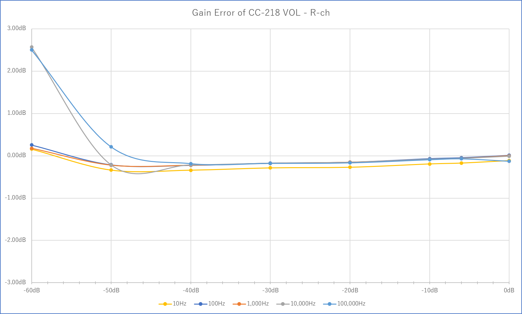 |
| CC-218 VOL gain deviation -- R-ch Input: DAC, Output: PRE OUT Horizontal axis: target gain, Vertical axis: difference between the target gain and the measured gain When the target gain is -50dB or lower, deviation increases at 10kHz or higher. The gain of -50dB or lower is so small volume and unused in actual situation, so the deviation is acceptable. When the target gain is -40dB or higher, deviation falls within -0.34dB to 0dB. |
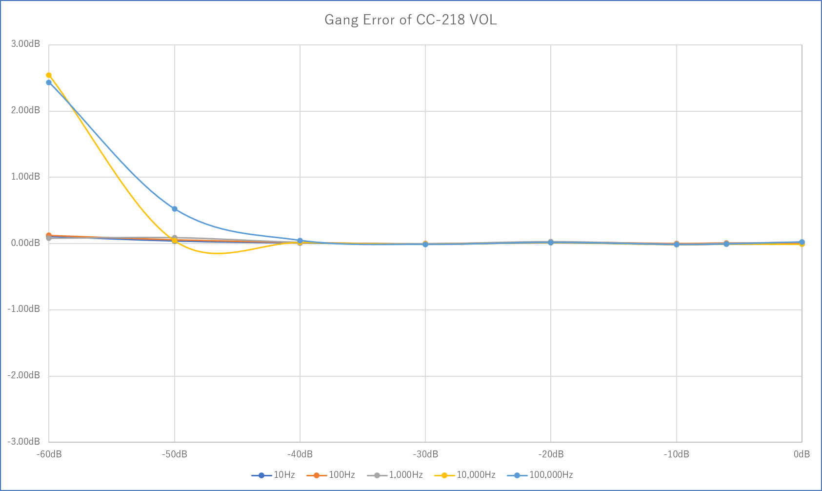 |
| CC-218 VOL channnel deviation (gang error) Input: DAC, Output: PRE OUT Horizontal axis: target gain, Vertical axis: difference in gain between channels (gang error) At target gain of -50dB or lower and frequency of 10kHz or higher, there appears gang error due to the deviation in R-ch. For target gain of -40 dB or higher, the deviation remains within -0.01 dB to +0.05 dB, which can be considered essentially zero gang error. |
An unexpected result was observed: only the right channel showed larger deviations at low target gains. However, since the deviation was within an acceptable range, I didn't make any modifications.
FFT analysis
Previously, I used FFT analysis to calculate and publish values such as
THD (Total Harmonic Distortion) and SNR (signal-to-noise ratio). However,
since this method differs from industry-standard measurement practices,
I believe it may not be helpful for readers. Therefore, only the spectrum
is shown here. Though the figure displays values for SNR and THD, please
disregard those numbers.
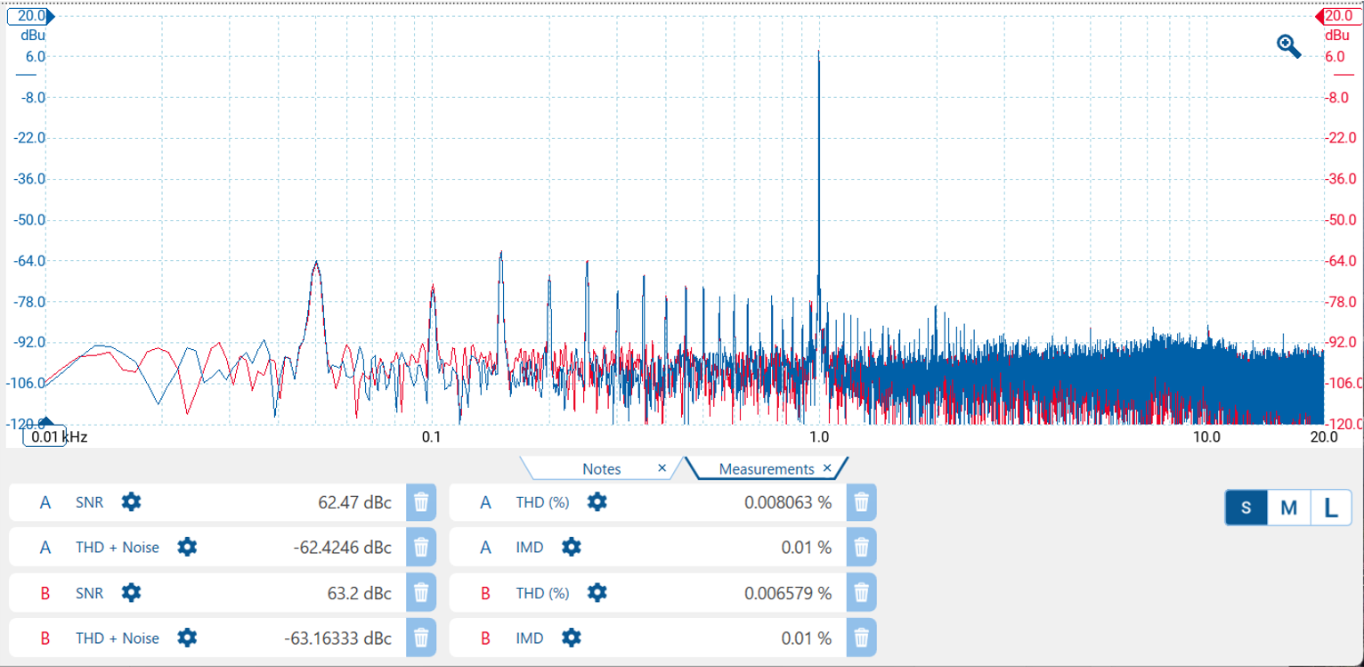 |
| CC-218 FFT analysis -- 1kHz Blue: input (DAC), Red: output (PRE OUT) The input and output waveforms are almost identical, indicating that the DUT produces virtually no distortion—neither low-order nor high-order harmonics. |
Charisteristics in Time Domain
Square wave response
The 10kHz square wave response is shown. The rising/falling edges are rounded
due to the input/output filters, but the waveform is as expected.
For reference, the waveform without filters is also shown.
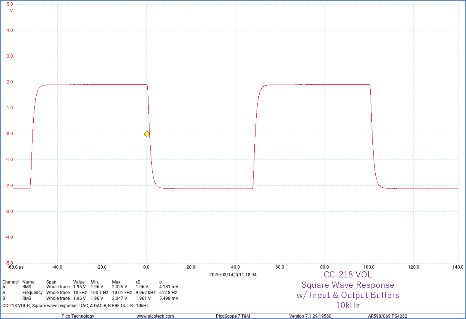 |
| CC-218 VOL Rev.B square wave response -- 10kHz, w/ input/output filters Though the rising/falling edges are rounded due to the effect of the filters, the waveform still appears beautiful. |
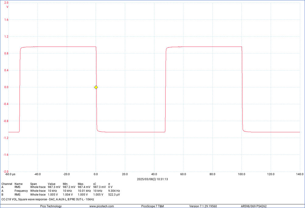 |
| CC-218 VOL square wave response -- 10kHz, w/o input/output filters Beautiful waveform; no overshooting, no ringing |
Adjustment of Power Indicators
The idea was to illuminate the inside of the enclosure with an LED, allowing
the light to leak out through the clear screws. However, it turned out
that the light was far too dim, and the screws wouldn’t appear to glow
unless the room was completely dark.
I then adjusted the setup so that the LED light shines directly on the
screws.
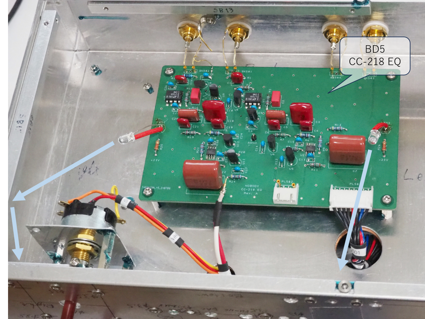 |
| Adjustment of power indicators -- CH2: AMP_EQ (1) LEDs on BD5 were changed. The LEDs' leads are not cut short. One of the leads is covered with insulation tube (2) After BD5 is installed in CH2, the directions of the LEDs are adjusted so that the lights shine on the clear screws. |
I did the same thing on CH1 (AMP_VOL); changed the LEDs on BD4 (CC-218
VOL Rev.B) and adjusted the directions of the LEDs.
My Own Review
As I always say, the builder's own evaluation immediately after completing his/her project is not reliable. Ideally, it should be evaluated after using it extensively for one or two years, but since I can't wait that long, I'm going to go ahead and write this anyway. Please feel free to take the following comments with a grain of salt.
I designed CC-218 with the goal of creating the ideal preamplifier, and
I’m confident that I was able to achieve that to a considerable extent.
However, I’m not fully satisfied with the appearance. This has reminded
me once again that I can’t hold a candle to professional designers. Since
I’m not very skilled with intricate craftsmanship, aesthetics will remain
an important challenge going forward.
Aside from the appearance, I’m more than satisfied with every other aspect.
I’m 100% satisfied with SQ (sound quality). As for functionality and usability,
CC-218 meets all of my own demanding requirements, so I truly believe there
isn’t a better preamp to be found anywhere in the world.
Overall score: 90 out of 100 points
Appearance
The area I put the most effort into for this project was the appearance
design.
I feel that the actual work doesn’t look quite as cool as the design renderings,
but overall, I’m fairly pleased with it. Up close, some imperfections are
noticeable, but from a distance, I think it looks pretty good.
If I were to give it a score, I’d say around 85 points."
Dress-Up Amplifier (detachable Front Panels)
One of the key features I focused on in this project is the 'dress-up amplifier'
concept. Front Panels are designed to be detachable, allowing the user
to select one from multiple designs according to his mood at the time.
This feature really saved me. The first stickers I made (ST1 and ST2) didn’t
have quite the level of quality I was hoping for, but ST1'' and ST2'',
while not exactly luxurious, give a much more refined impression—so I went
with those instead.
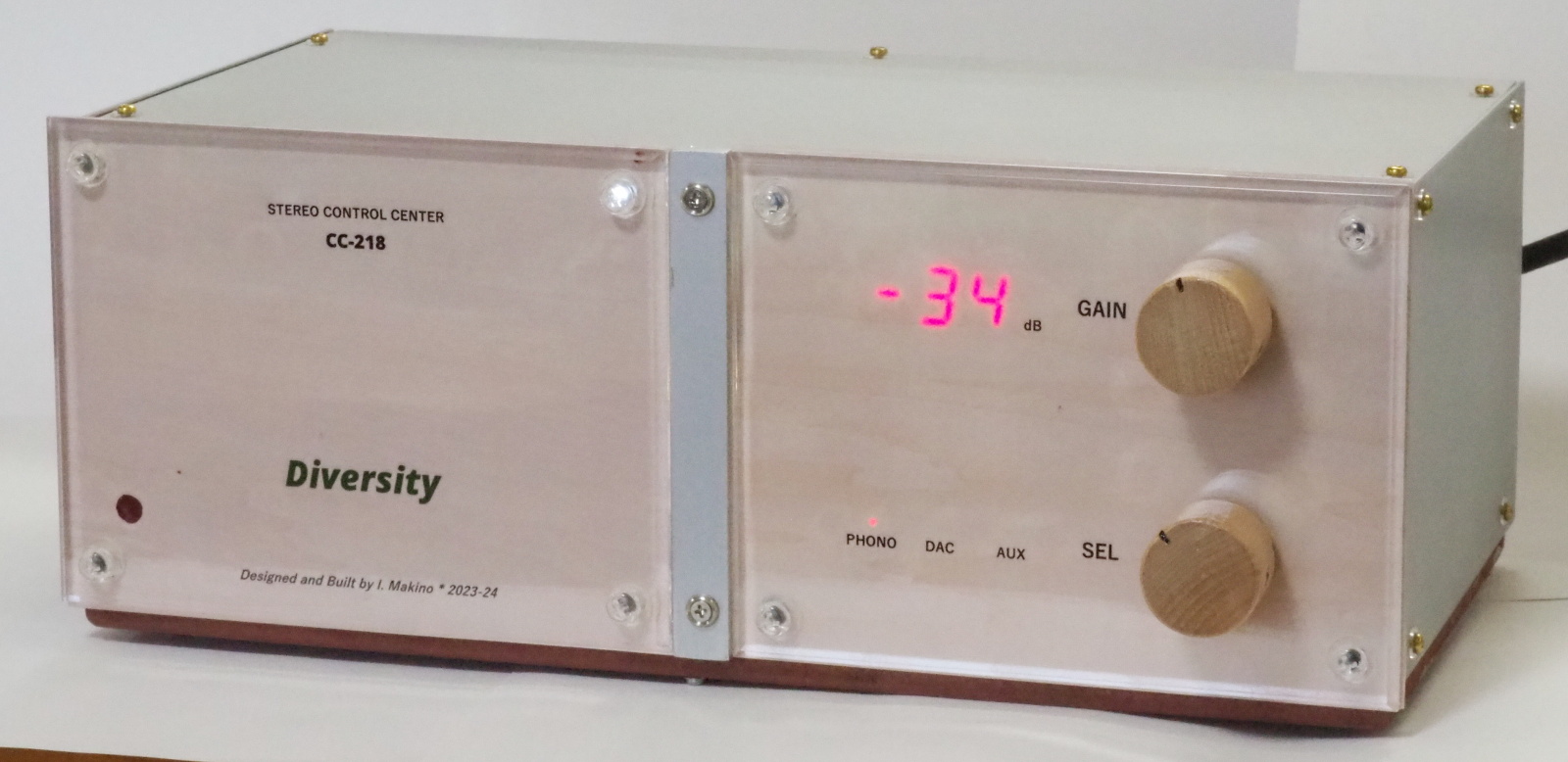 |
 |
| Front panel stickers: ST1, ST2 Grain of wood (sino) |
Front panel stickers: ST1', ST2' Marble |
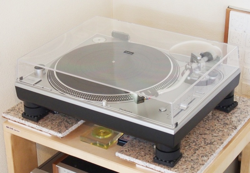 |
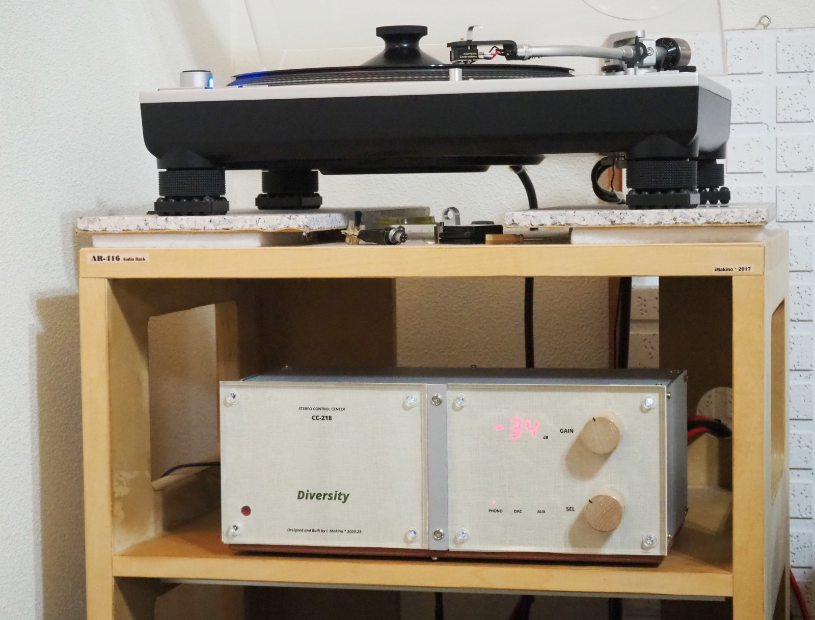 |
| Front panel stickers: ST1'', ST2'' Canvas My favorite one; my current selection |
Front panel stickers: ST1'', ST2'' Canvas The color of the stickers is a bit different from that in the left photo due to the difference of the settings of the camera The color in this photo is closer to the actual color. (I think) this color (canvas) goes with the audio rack (AR-416). |
Poor craft concerning appearance
I made another blunder with painting, which I'm not good at. I don't plan
to repaint it for now, but I intend to give it a try once I regain the
motivation.
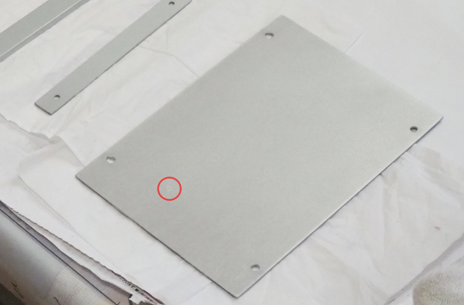 |
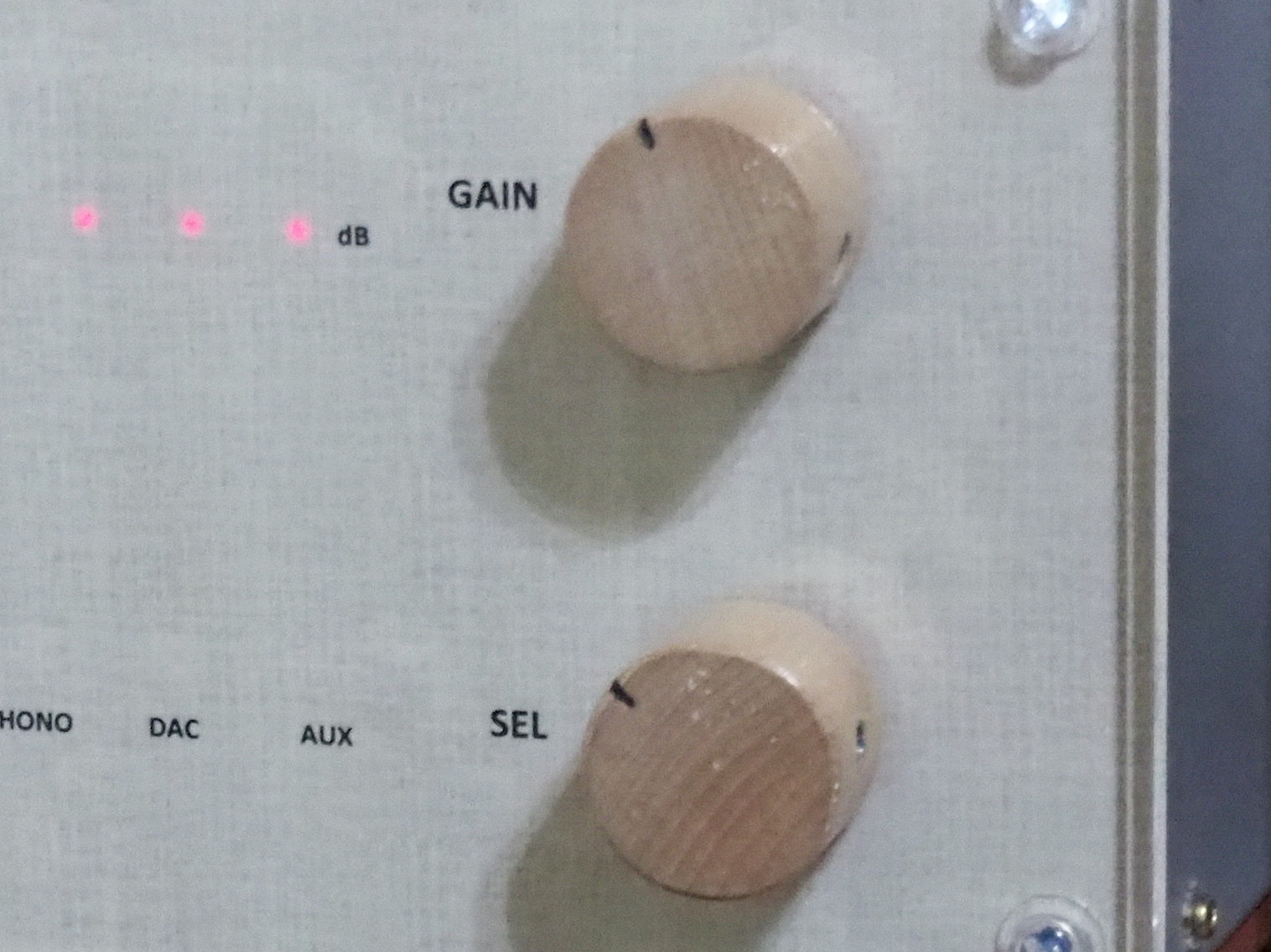 |
| Painting Failure – Exterior Panel – PN6: Side Panel L Some areas have exposed bare metal (circled in red). The finish is uneven overall and lacks gloss. The same applies to the other exterior panels as well. |
Painting Failure – Knobs I wanted a light, natural wood finish, but the color ended up too dark. I should have used wood wax like I did with AR-416. The white spots are caused by bubbles that formed during painting. |
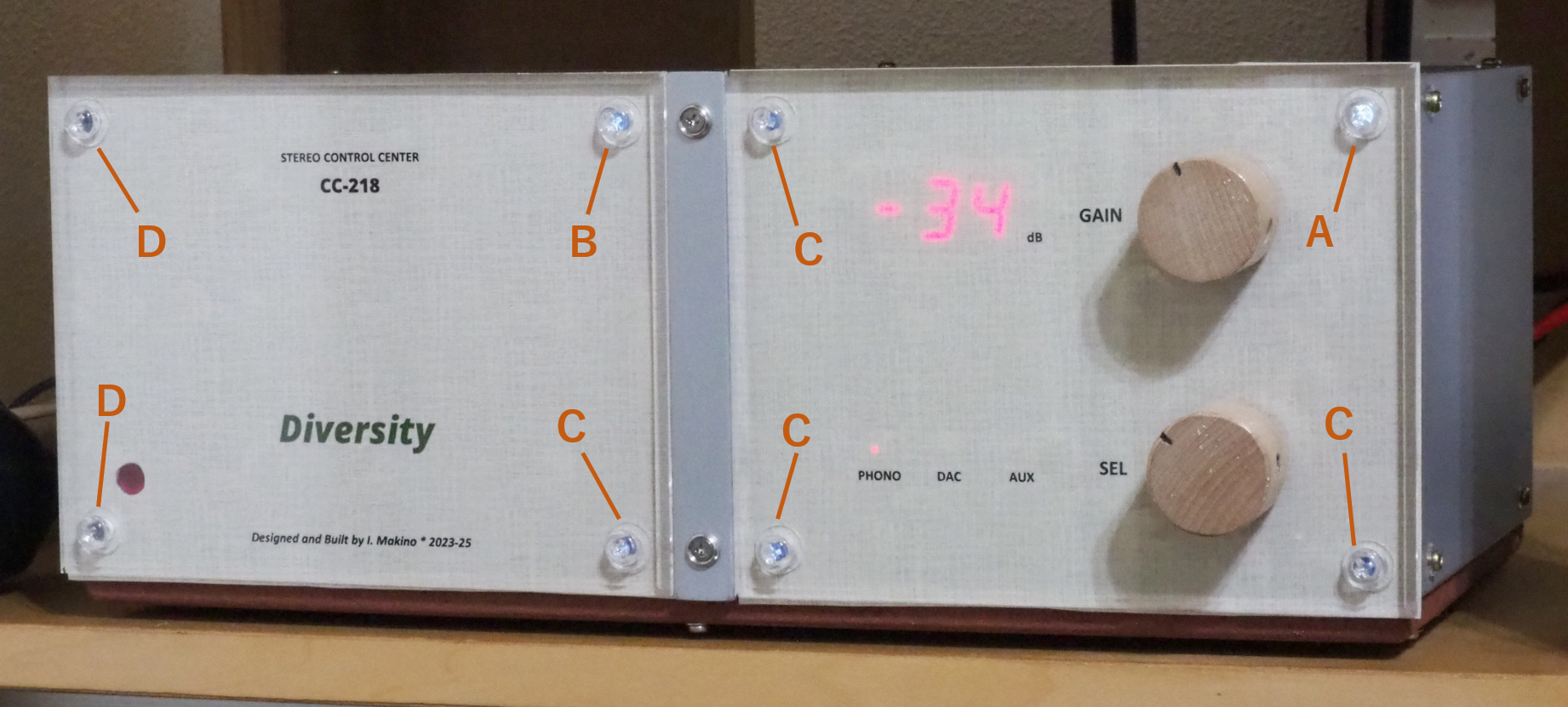 |
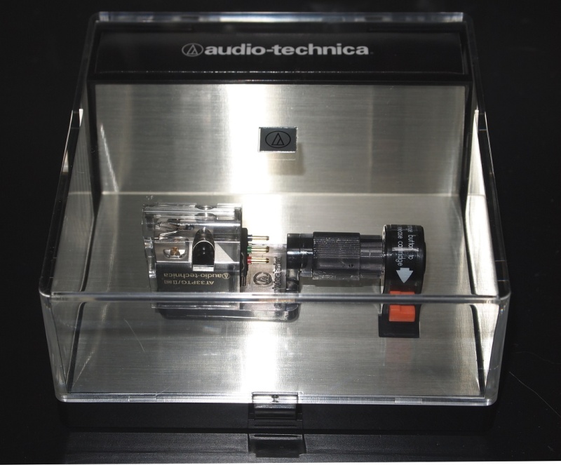 |
| Power Indicators I'm using clear screws as substitutes for indicators, but the brightness is inconsistent. I didn’t properly plan the LED placement. A: Bright, B: Fairly bright C: Dim (visible if the room is somewhat dark) D: Very dim (only visible if the room is completely dark) |
Front Panel Sticker: ST2'' The sticker was misaligned when applied, so the lettering doesn’t match the position of the LEDs. It’s shifted 1.5mm downward and 1.5mm to the right. It’s a small mistake, but since it catches my eye every time I operate the preamp, it’s quite irritating. |
Sound Quality
I believe the sound quality (SQ) has been dramatically improved compared
to my previous preamp (PA-210).
What stands out most is the spatial imaging. The soundstage has become
more coherent, with precise and stable localization.
I used to think the blurred imaging was due to the room’s acoustics, but
I’ve realized that 60–70% of it was actually caused by the preamp.
The reason is that the PA-210 is a tube preamp, and it has a tendency to
convert acoustic feedback from the speakers into electrical signals (the
so-called microphonic noise), whereas the CC-218, being a solid-state preamp,
doesn’t have that characteristic.
In fact, when listening through headphones, the sound quality difference
between the CC-218 and PA-210 isn’t that significant. This really made
me realize just how detrimental microphonic noise can be.
Previously, I wrote on this website that “I’m not particular about pinpoint localization,” but I’d like to retract that statement. I’ve come to realize that precise and stable localization truly enhances the comfort and enjoyment of listening to music.
The low noise level is another major difference compared to my previous
preamp. Even when selecting PHONO input and turning the volume all the
way up, there’s absolutely no noise—it's an incredibly satisfying experience.
This is the sixth preamp I’ve built, and it’s deeply moving to feel that
I’ve finally reached this level.
I believe this is thanks to the effectiveness of the ground planes on the
PCBs, which provides an unwavering ground, like the earth itself.
In addition, the precise operation—such as the good linearity of the volume (gain) control, the minimal gang error, and the low RIAA deviation—also contributes to a sense of reliability and confidence when listening to music.
In the Gaudi II system, six amplifiers (or eight if you count the balanced/unbalanced converters) are used simultaneously, and I didn’t expect SQ to improve this much just by replacing a single unit. It was a pleasant surprise.
This is something I always notice whenever I improve a part of the system,
and this time was no exception—I felt that SQ of vinyls improved significantly
more than that of digital sources.
Large ensembles like orchestras and big bands sounded especially better.
I’ve had several pleasant surprises where vinyls that hadn’t sounded very
good before turned out to have excellent SQ when I listened to them again
after a long time.
Many people seek a retro sound from vinyls—a soft, warm, somewhat blurry
tone—but the analog sound from the Gaudi II system gives a vivid and lifelike
impression instead.
User-friendliness
Usability
I defined the operation specifications to fully satisfy my own demanding
requirements, and since both the hardware and firmware were designed accordingly,
I have no complaints at all when it comes to usability.
In particular, adopting the TV infrared remote and making full use of its
many buttons was an excellent decision. With remotes that only have VOL+
and VOL– buttons, it’s difficult to make quick adjustments. The gain preset
function in this preamp has proven to be extremely useful.
Choosing 0.5dB steps for gain adjustment was also the right decision. Since
volume and sound quality are closely related, being able to fine-tune in
0.5dB steps allows for precise control. MV-217 uses 2dB steps, but that
makes it difficult to set the optimal volume.
| Preset Function Quickly adjust to the optimal volume using the preset function. |
Mute Function Fade-out when muting, fade-in when unmuting. |
Using the variable resistor instead of a rotary encoder for the panel volume
knob was also an excellent choice.
The operability is exactly the same as a pure analog amplifier. Especially
if the LED display is turned off, you can’t tell it apart from a pure analog
amp. This makes operating it very comfortable when playing vinyls.
Regarding usability, I give it 120 points.
It’s the only preamp in the world that completely satisfies me.
Other aspects in user-friendliness
The size and shape are just right, making installation easy.
PA-210 used a separate power supply unit (AC adapter), which was inconvenient
during setup and maintenance. CC-218 has a built-in power supply and uses
a power cord plugged into an inlet, allowing for stress-free maintenance.
Thorough measures were taken to reduce power supply noise, and because of the high regulation, SQ is not affected even if the AC line quality is poor. This is another reason the unit can be used with confidence. Moreover, in the Gaudi II/III systems, power is supplied from a power distributor equipped with double filtering, providing clean AC power.
Component Selection
Electronic volume chip
The reason for choosing TI’s PGA2310 was that it requires no external components
and is easy to use. In terms of sound quality as well, there didn’t seem
to be any issues according to the datasheet, so it was adopted.
I did briefly consider using JRC’s MUSES72320, with which I was satisfied
in MV-217 project, but I avoided it because it requires many external components.
Now that I think about it, since MUSES has more thorough noise countermeasures,
I feel I should have chosen MUSES instead.
As mentioned earlier, when CC-218 is used in combination with the TEAC AP-505, pop noise can be heard when changing the gain. However, no such noise is heard when the MV-217 is paired with the AP-505. It is clear that the MUSES72320 has lower noise.
MCU chip
I believe choosing PIC18F2520 was the right decision.
Since amplifier firmware is simple in general, an 8-bit MCU is more than
sufficient. PIC18F2520 has all the necessary peripherals built in, including
the clock oscillator circuit and the reset circuit. The number of general-purpose
I/O ports, memory capacity, and other specifications are all just right.
I'm also satisfied with MPLAB X IDE, which is a user-friendly development
tool.
AC/DC converter
At first, I chose a basic AC/DC converter (CUI PSK-10D-5-T) for the digital
circuitry. I assumed it would be fine since it was just for digital use
and didn’t think much of it.
But when I actually powered it on, I was shocked—it emitted intense radiated
noise. You may experience that you hear a loud, harsh noise when placing
an AM radio next to an AC adapter. That's the same kind of noise.
I came to realize that only high-spec AC/DC converters designed for medical
equipment are suitable for audio amplifiers.
PCB
I ordered all the PCBs from the Chinese manufacturer, JLCPCB.
What surprised me most was how inexpensive they were. Even the largest
board, CC-218 VOL, cost only about 400 JPY per unit. It’s hard to believe
it’s cheaper than a general-purpose board from Sunhayato. That said, the
minimum order quantity is five boards, so in reality, it costs about 2,000
JPY plus shipping (around $9). All payments are made in US dollars, so
the total cost is affected by exchange rates.
As for quality, although I haven’t compared it directly with products from other companies, I think it’s very good. The boards are properly manufactured according to the 1 μm design rules, and in actual use, there haven’t been any issues at all.
Placing an order is also easy. You just fill out the required fields on
the order form on their website and upload your design data (Gerber files).
Unlike Japanese companies, they don’t care whether the customer is a company
or an individual. When registering as a user, there’s a field to enter
your occupation, and since “Hobbyist” was one of the options, I selected
that.
Once the order is accepted, the review process begins immediately and is
completed in about 10 minutes (clearly without any human involvement).
The boards are finished and shipped the next day or the day after. PCBs
are delivered so effortlessly that it almost feels like buying them from
a vending machine.
Other aspects
4-channel stereo
To support 4-channel stereo, I built in a matrix circuit that generates
signals for the rear speakers. It’s not fully compatible with the Sansui
QS 4-channel system—in a sense, it’s more of a pseudo-4-channel—but it
still produced a noticeable effect. You can clearly hear sound images that
should be positioned behind coming from the rear.
Listening to Sansui’s demo record (LP: Kei Ogura – Seishun no Uta, SANSUI QSD-2002) gives a sense of rapture, as if being drawn into a unique
miniature universe. Kei Ogura’s early hit songs are enhanced with orchestral
intros, sound effects like steam locomotives, or the sound of raindrops,
and these elements seem to bring out his world even more than just his
vocals alone.
When I show CC-218 to friends, this vinyl always pleases them most.
PCB design
It was my first time designing PCBs, but I think I did a pretty good job.
Including the circuit design, there weren’t any major bugs, which made
debugging the firmware go smoothly. Thoroughly verifying operation through
simulation really paid off.
EMI
When incorporating digital circuits, one concern is EMI (Electro-Magnetic
Interference).
I don’t have the equipment to measure conducted noise on the AC line, but
since I’m using a medical-grade AC/DC converter, it should comply with
EN55032/11 Class B standards.
While I also can’t measure radiated noise, a simple test using an AM radio
revealed that it emits very little interference. When bringing the radio
close to the MCU compartment (on the left side when viewed from the front),
only a faint noise can be heard. It’s at a lower level than that of the
Technics SL-1200GR.
Summing-up
Although I did repeat a few minor mistakes I had done before, overall, I think I did a good job.
I built my first preamp in 1973, when I was 16 years old. Now, at 68, I’ve finally created a preamp I’m truly satisfied with. I don’t think I’ll be making another one. I intend to keep using CC-218 Diversity for the rest of my life.
By taking on new technologies—such as creating my original PCBs, implementing
GND planes, and adding infrared remote control—I was able to overcome various
challenges. I’m glad I took on the challenge.
In particular, acquiring PCB design skills was a major achievement. If
I can keep the energy and motivation, I’d like to use the skills I’ve gained
this time to take on the challenge of building a digital crossover network.